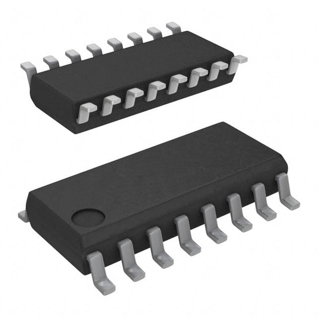
Xem thông số kỹ thuật để biết chi tiết sản phẩm.

CD74HC138M96E4
Product Overview
- Category: Integrated Circuit
- Use: Decoding and demultiplexing
- Characteristics: High-speed operation, low power consumption
- Package: SOIC-16
- Essence: 3-to-8 line decoder/demultiplexer
- Packaging/Quantity: Tape and reel, 2500 units per reel
Specifications
- Supply Voltage Range: 2V to 6V
- High-Level Input Voltage: 2V to VCC
- Low-Level Input Voltage: GND to 0.8V
- High-Level Output Current: -4mA
- Low-Level Output Current: 4mA
- Operating Temperature Range: -40°C to +85°C
Detailed Pin Configuration
The CD74HC138M96E4 has a total of 16 pins, which are labeled as follows:
- A0 (Address input)
- A1 (Address input)
- A2 (Address input)
- G2A (Enable input)
- Y7 (Output)
- Y6 (Output)
- Y5 (Output)
- Y4 (Output)
- Y3 (Output)
- Y2 (Output)
- Y1 (Output)
- Y0 (Output)
- G1 (Enable input)
- G2B (Enable input)
- VCC (Supply voltage)
- GND (Ground)
Functional Features
The CD74HC138M96E4 is a 3-to-8 line decoder/demultiplexer integrated circuit. It takes three address inputs (A0, A1, and A2) and enables the corresponding output line based on the binary value of the address inputs. The enable inputs (G1 and G2A/G2B) control the operation of the decoder/demultiplexer.
Advantages and Disadvantages
Advantages: - High-speed operation - Low power consumption - Compact SOIC-16 package - Wide supply voltage range
Disadvantages: - Limited number of address inputs (3 bits) - Output current limitations (-4mA to 4mA)
Working Principles
The CD74HC138M96E4 uses a combination of logic gates to decode the address inputs and enable the appropriate output line. When the enable inputs are activated, the decoder/demultiplexer selects the corresponding output based on the binary value of the address inputs. The selected output line is then driven to either a high or low logic level.
Detailed Application Field Plans
The CD74HC138M96E4 can be used in various applications, including but not limited to: 1. Address decoding in microcontrollers and microprocessors 2. Memory selection in digital systems 3. Data routing in communication systems 4. Multiplexing and demultiplexing in data transmission 5. Control signal generation in industrial automation
Detailed and Complete Alternative Models
- SN74LS138N: Similar 3-to-8 line decoder/demultiplexer with TTL logic levels.
- CD4514BE: 4-to-16 line decoder/demultiplexer with latch enable feature.
- 74HC238: 3-to-8 line decoder/demultiplexer with active-low outputs.
These alternative models provide similar functionality to the CD74HC138M96E4 and can be used as replacements depending on specific requirements.
In conclusion, the CD74HC138M96E4 is a versatile integrated circuit that offers high-speed decoding and demultiplexing capabilities. Its compact package and wide supply voltage range make it suitable for various applications in digital systems. However, its limited number of address inputs and output current limitations should be considered when designing circuits.
Liệt kê 10 câu hỏi và câu trả lời thường gặp liên quan đến ứng dụng CD74HC138M96E4 trong giải pháp kỹ thuật
Sure! Here are 10 common questions and answers related to the application of CD74HC138M96E4 in technical solutions:
Q: What is CD74HC138M96E4? A: CD74HC138M96E4 is a 3-to-8 line decoder/demultiplexer integrated circuit (IC) that can be used in various digital logic applications.
Q: What is the purpose of CD74HC138M96E4? A: The purpose of CD74HC138M96E4 is to decode a binary input and select one of the eight output lines based on the input value.
Q: What voltage levels does CD74HC138M96E4 support? A: CD74HC138M96E4 supports voltage levels ranging from 2V to 6V, making it compatible with both TTL and CMOS logic families.
Q: How many inputs does CD74HC138M96E4 have? A: CD74HC138M96E4 has three binary inputs (A0, A1, and A2) that determine which output line is selected.
Q: How many output lines does CD74HC138M96E4 have? A: CD74HC138M96E4 has eight output lines (Y0-Y7) that can be individually selected based on the input values.
Q: Can CD74HC138M96E4 be cascaded to increase the number of output lines? A: Yes, multiple CD74HC138M96E4 ICs can be cascaded together to increase the number of output lines by using the outputs of one IC as inputs for another.
Q: What is the maximum current that CD74HC138M96E4 can source or sink? A: CD74HC138M96E4 can source or sink up to 4mA of current per output pin.
Q: Can CD74HC138M96E4 be used in both active-high and active-low applications? A: Yes, CD74HC138M96E4 can be used in both active-high and active-low applications by appropriately connecting the enable (E) pin.
Q: What is the propagation delay of CD74HC138M96E4? A: The typical propagation delay of CD74HC138M96E4 is around 13ns, making it suitable for high-speed applications.
Q: Are there any specific precautions to consider when using CD74HC138M96E4? A: It is important to ensure that the power supply voltage does not exceed the specified limits (2V to 6V) and to avoid exceeding the maximum current ratings for the IC.
Please note that these answers are general and may vary depending on the specific application and requirements.

