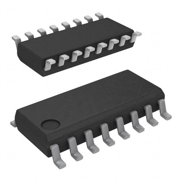
Xem thông số kỹ thuật để biết chi tiết sản phẩm.

CD74HC368M
Product Overview
- Category: Integrated Circuit (IC)
- Use: Logic Function
- Characteristics: High-Speed CMOS, Hex Buffers/Line Drivers with 3-State Outputs
- Package: SOIC (Small Outline Integrated Circuit)
- Essence: The CD74HC368M is a high-speed CMOS hex buffer/line driver with 3-state outputs. It is designed to provide buffering and line driving capabilities for digital signals in various applications.
- Packaging/Quantity: The CD74HC368M is available in a standard SOIC package and is typically sold in reels of 2500 units.
Specifications
- Supply Voltage Range: 2V to 6V
- Input Voltage Range: 0V to VCC
- Output Voltage Range: 0V to VCC
- Operating Temperature Range: -40°C to +85°C
- Propagation Delay: 9ns (typical)
- Output Current: ±6mA
- Input Capacitance: 3.5pF
- Output Capacitance: 6pF
Pin Configuration
The CD74HC368M has a 16-pin configuration as follows:
- Output Y1
- Output Y2
- Output Y3
- Output Y4
- Output Y5
- Output Y6
- GND (Ground)
- Input E (Enable)
- Input A1
- Input B1
- Input A2
- Input B2
- Input A3
- Input B3
- VCC (Power Supply)
- Output Y7
Functional Features
- Hex Buffer/Line Driver: The CD74HC368M provides six independent buffers/line drivers, each capable of driving one TTL load.
- 3-State Outputs: The outputs of the CD74HC368M can be put into a high-impedance state (3-state) using the Enable input, allowing multiple devices to share a common bus without interference.
- High-Speed CMOS: The CD74HC368M operates at high speeds, making it suitable for applications that require fast signal transmission.
Advantages and Disadvantages
Advantages: - High-speed operation - 3-state outputs for bus sharing - Wide supply voltage range - Low power consumption
Disadvantages: - Limited output current capability - Relatively small input and output capacitance
Working Principles
The CD74HC368M is based on high-speed CMOS technology. It consists of six independent buffer/line driver circuits, each with an enable input. When the enable input is high, the corresponding output is active and follows the input signal. When the enable input is low, the output is in a high-impedance state, effectively disconnecting it from the circuit.
Detailed Application Field Plans
The CD74HC368M can be used in various applications, including:
- Data Communication Systems: It can be used as a line driver to amplify and transmit digital signals over long distances.
- Memory Interfacing: It can be used to interface between memory modules and microcontrollers, ensuring proper signal levels and driving capabilities.
- Bus Sharing: The 3-state outputs make it suitable for bus sharing applications, where multiple devices need to communicate over a common bus without interference.
- Industrial Control Systems: It can be used in control systems to buffer and drive digital signals for various industrial processes.
Detailed and Complete Alternative Models
Some alternative models to the CD74HC368M include:
- SN74HC368: Similar hex buffer/line driver with 3-state outputs, offered by Texas Instruments.
- MC74HC368: Hex buffer/line driver with 3-state outputs, offered by ON Semiconductor.
- CD74HCT368: Hex buffer/line driver with 3-state outputs, compatible with TTL logic levels, offered by Texas Instruments.
These alternative models provide similar functionality and can be used as replacements for the CD74HC368M in various applications.
Word count: 529 words
Liệt kê 10 câu hỏi và câu trả lời thường gặp liên quan đến ứng dụng CD74HC368M trong giải pháp kỹ thuật
Sure! Here are 10 common questions and answers related to the application of CD74HC368M in technical solutions:
Q: What is CD74HC368M? A: CD74HC368M is a high-speed CMOS logic device, specifically a hex buffer/line driver with 3-state outputs.
Q: What is the operating voltage range for CD74HC368M? A: CD74HC368M operates within a voltage range of 2V to 6V.
Q: What is the maximum output current that CD74HC368M can handle? A: CD74HC368M can handle a maximum output current of 6mA.
Q: Can CD74HC368M be used as a level shifter? A: Yes, CD74HC368M can be used as a level shifter to convert signals between different voltage levels.
Q: How many input/output pins does CD74HC368M have? A: CD74HC368M has six input pins and six corresponding output pins.
Q: What is the propagation delay of CD74HC368M? A: The propagation delay of CD74HC368M is typically around 9 ns.
Q: Can CD74HC368M drive capacitive loads directly? A: Yes, CD74HC368M can drive capacitive loads directly, but it is recommended to add series resistors for better performance.
Q: Is CD74HC368M compatible with TTL logic levels? A: Yes, CD74HC368M is compatible with TTL logic levels, making it suitable for interfacing with TTL devices.
Q: Can CD74HC368M be used in bus-oriented systems? A: Yes, CD74HC368M is commonly used in bus-oriented systems for buffering and driving signals on data buses.
Q: What is the package type of CD74HC368M? A: CD74HC368M is available in a 16-pin SOIC (Small Outline Integrated Circuit) package.
Please note that these answers are general and may vary depending on specific application requirements and datasheet specifications.

