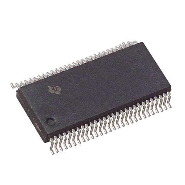
Xem thông số kỹ thuật để biết chi tiết sản phẩm.

CY74FCT16543CTPVC
Basic Information Overview
- Category: Integrated Circuit (IC)
- Use: Data storage and transfer
- Characteristics: High-speed, low-power consumption
- Package: TSSOP (Thin Shrink Small Outline Package)
- Essence: 16-bit registered transceiver
- Packaging/Quantity: Tape and Reel, 2500 units per reel
Specifications
- Number of Bits: 16
- Logic Family: FCT (Fast CMOS TTL)
- Supply Voltage: 4.5V to 5.5V
- Input/Output Type: Tri-State
- Operating Temperature Range: -40°C to +85°C
- Propagation Delay: 3.8ns (typical)
- Output Drive Capability: ±24mA
Detailed Pin Configuration
- A1: Data Input/Output 1
- B1: Data Input/Output 2
- A2: Data Input/Output 3
- B2: Data Input/Output 4
- A3: Data Input/Output 5
- B3: Data Input/Output 6
- A4: Data Input/Output 7
- B4: Data Input/Output 8
- A5: Data Input/Output 9
- B5: Data Input/Output 10
- A6: Data Input/Output 11
- B6: Data Input/Output 12
- A7: Data Input/Output 13
- B7: Data Input/Output 14
- A8: Data Input/Output 15
- B8: Data Input/Output 16
- GND: Ground
- OE: Output Enable
- CLK: Clock Input
- LE: Latch Enable
- A9: Data Input/Output 17
- B9: Data Input/Output 18
- A10: Data Input/Output 19
- B10: Data Input/Output 20
- A11: Data Input/Output 21
- B11: Data Input/Output 22
- A12: Data Input/Output 23
- B12: Data Input/Output 24
- A13: Data Input/Output 25
- B13: Data Input/Output 26
- A14: Data Input/Output 27
- B14: Data Input/Output 28
- A15: Data Input/Output 29
- B15: Data Input/Output 30
- A16: Data Input/Output 31
- B16: Data Input/Output 32
- VCC: Supply Voltage
Functional Features
- Bidirectional data transfer between two independent buses
- Output enable and latch enable control for flexible operation
- Tri-state outputs for bus sharing capability
- High-speed operation suitable for data storage and transfer applications
- Low power consumption for energy-efficient designs
Advantages
- High-speed performance allows for efficient data transfer
- Low power consumption helps in reducing energy usage
- Tri-state outputs enable bus sharing, optimizing resource utilization
- Wide operating temperature range enables usage in various environments
- Compact TSSOP package facilitates space-saving designs
Disadvantages
- Limited number of bits (16) may not be sufficient for certain applications requiring larger data storage or transfer capacity
- Requires external clock and control signals for proper operation
- Not compatible with all logic families, limiting interoperability options
Working Principles
The CY74FCT16543CTPVC is a 16-bit registered transceiver that allows bidirectional data transfer between two independent buses. It operates based on clock and control signals provided externally. The output enable (OE) and latch enable (LE) pins control the direction of data flow and the storage of data, respectively. Tri-state outputs enable bus sharing by allowing multiple devices to connect to the same bus without interfering with each other.
Detailed Application Field Plans
- Data communication systems
- Microprocessor-based systems
- Networking equipment
- Industrial automation
- Automotive electronics
- Consumer electronics
Detailed and Complete Alternative Models
- SN74FCT16543CTPVC
- MC74FCT16543CTPVC
- CD74FCT16543CTPVC
- 74FCT16543CTPVC
- NTE74FCT16543CTPVC
These alternative models offer similar functionality and characteristics to the CY74FCT16543CTPVC, providing options for different manufacturers or availability.
Word count: 527 words
Liệt kê 10 câu hỏi và câu trả lời thường gặp liên quan đến ứng dụng CY74FCT16543CTPVC trong giải pháp kỹ thuật
Sure! Here are 10 common questions and answers related to the application of CY74FCT16543CTPVC in technical solutions:
Q: What is CY74FCT16543CTPVC? A: CY74FCT16543CTPVC is a type of integrated circuit (IC) that functions as a 16-bit transparent latch with 3-state outputs.
Q: What are the typical applications of CY74FCT16543CTPVC? A: CY74FCT16543CTPVC is commonly used in various digital systems, such as data storage, address decoding, bus interfacing, and general-purpose logic.
Q: What is the operating voltage range for CY74FCT16543CTPVC? A: The operating voltage range for CY74FCT16543CTPVC is typically between 4.5V and 5.5V.
Q: How many output pins does CY74FCT16543CTPVC have? A: CY74FCT16543CTPVC has 16 output pins, each capable of driving a standard TTL load.
Q: Can CY74FCT16543CTPVC be used in high-speed applications? A: Yes, CY74FCT16543CTPVC is designed to operate at high speeds, making it suitable for applications requiring fast data transfer.
Q: Does CY74FCT16543CTPVC support bidirectional data flow? A: No, CY74FCT16543CTPVC is a unidirectional latch, meaning it can only store and output data in one direction.
Q: What is the maximum clock frequency supported by CY74FCT16543CTPVC? A: The maximum clock frequency supported by CY74FCT16543CTPVC is typically in the range of 100MHz to 150MHz.
Q: Can CY74FCT16543CTPVC be cascaded to increase the number of latches? A: Yes, multiple CY74FCT16543CTPVC ICs can be cascaded together to increase the number of latches and create larger data storage systems.
Q: Does CY74FCT16543CTPVC have any built-in protection features? A: Yes, CY74FCT16543CTPVC includes built-in ESD (electrostatic discharge) protection on all inputs and outputs.
Q: What package options are available for CY74FCT16543CTPVC? A: CY74FCT16543CTPVC is available in various package options, such as TSSOP (Thin Shrink Small Outline Package) and LQFP (Low-Profile Quad Flat Package).
Please note that the specific details and specifications may vary depending on the manufacturer and version of the CY74FCT16543CTPVC IC.

