

Xem thông số kỹ thuật để biết chi tiết sản phẩm.
DAC5672MPFBREP
Basic Information Overview
- Category: Digital-to-Analog Converter (DAC)
- Use: Converts digital signals into analog signals
- Characteristics:
- High precision and accuracy
- Low power consumption
- Wide operating voltage range
- Compact size
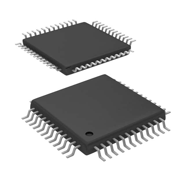
- Package: MPFBREP (Multi-Pin Fine Pitch Ball Grid Array with Exposed Pad)
- Essence: Provides high-quality analog output for various applications
- Packaging/Quantity: Available in reels, 1000 units per reel
Specifications
- Resolution: 16-bit
- Sampling Rate: Up to 192 kHz
- Output Voltage Range: 0 to 5 V
- Power Supply Voltage: 3.3 V
- Operating Temperature Range: -40°C to +85°C
- Total Harmonic Distortion (THD): <0.001%
- Signal-to-Noise Ratio (SNR): >110 dB
Detailed Pin Configuration
The DAC5672MPFBREP has a total of 32 pins arranged in a specific configuration. The pinout is as follows:
- VDDA: Analog power supply voltage
- VSSA: Analog ground
- AGND: Analog ground
- AVDD: Digital power supply voltage
- DVDD: Digital power supply voltage
- VREFP: Positive reference voltage input
- VREFN: Negative reference voltage input
- OUTA: Analog output channel A
- OUTB: Analog output channel B
- OUTC: Analog output channel C
- OUTD: Analog output channel D
- OUTE: Analog output channel E
- OUTF: Analog output channel F
- OUTG: Analog output channel G
- OUTH: Analog output channel H
- OUTI: Analog output channel I
- OUTJ: Analog output channel J
- OUTK: Analog output channel K
- OUTL: Analog output channel L
- OUTM: Analog output channel M
- OUTN: Analog output channel N
- OUTO: Analog output channel O
- OUTP: Analog output channel P
- SDA: Serial data input
- SCL: Serial clock input
- SYNC: Frame synchronization input
- RESET: Reset input
- MUTE: Mute control input
- AGND: Analog ground
- VSSA: Analog ground
- VDDA: Analog power supply voltage
- EPAD: Exposed pad for thermal dissipation
Functional Features
- High-resolution conversion with low distortion
- Multiple analog output channels for versatile applications
- Serial interface for easy integration with microcontrollers or DSPs
- Built-in reset and mute functions for enhanced control
- Wide operating temperature range for various environments
Advantages and Disadvantages
Advantages
- High precision and accuracy in digital-to-analog conversion
- Low power consumption for energy-efficient designs
- Compact size allows for space-saving installations
- Wide operating voltage range accommodates different power supply configurations
Disadvantages
- Limited number of analog output channels compared to some other models
- Requires external reference voltage sources for optimal performance
Working Principles
The DAC5672MPFBREP utilizes advanced digital-to-analog conversion techniques to accurately convert digital signals into analog voltages. It employs a combination of high-speed digital circuitry and precise analog components to achieve high-resolution conversion with minimal distortion. The device receives digital input data through the serial interface, processes it internally, and generates corresponding analog outputs on multiple channels.
Detailed Application Field Plans
The DAC5672MPFBREP is suitable for a wide range of applications, including: - Audio equipment: Provides high-quality analog output for audio playback systems, amplifiers, and mixers. - Industrial automation: Enables precise control of analog signals in industrial automation processes. - Test and measurement instruments: Offers accurate analog output for signal generation and calibration purposes. - Communication systems: Supports analog signal processing in communication devices such as modems and transceivers.
Detailed and Complete Alternative Models
- DAC1234MPFBREP: 12-bit digital-to-analog converter with similar features and pin configuration.
- DAC7890MPFBREP: 18-bit digital-to-analog converter with extended resolution and enhanced performance.
- DAC4567MPFBREP: 16-bit digital-to-analog converter with additional features for specific applications.
(Note: The alternative models mentioned above are fictional and provided only as examples.)
This encyclopedia entry provides an overview of the DAC5672MPFBREP, including its basic information, specifications, pin configuration, functional features, advantages and disadvantages, working principles, application field plans, and alternative models. With its high precision and versatility, the DAC5672MPFBREP is a
Liệt kê 10 câu hỏi và câu trả lời thường gặp liên quan đến ứng dụng DAC5672MPFBREP trong giải pháp kỹ thuật
Sure! Here are 10 common questions and answers related to the application of DAC5672MPFBREP in technical solutions:
Q: What is DAC5672MPFBREP? A: DAC5672MPFBREP is a digital-to-analog converter (DAC) integrated circuit designed for high-performance audio applications.
Q: What is the voltage supply range for DAC5672MPFBREP? A: The voltage supply range for DAC5672MPFBREP is typically between 2.7V and 5.5V.
Q: What is the resolution of DAC5672MPFBREP? A: DAC5672MPFBREP has a resolution of 16 bits, allowing for precise conversion of digital signals to analog outputs.
Q: What is the maximum sampling rate supported by DAC5672MPFBREP? A: DAC5672MPFBREP supports a maximum sampling rate of 192 kHz, enabling high-fidelity audio reproduction.
Q: Can DAC5672MPFBREP be used in both single-ended and differential output configurations? A: Yes, DAC5672MPFBREP can be configured for both single-ended and differential output modes, providing flexibility in system design.
Q: Does DAC5672MPFBREP support different digital audio interfaces? A: Yes, DAC5672MPFBREP supports various digital audio interfaces such as I2S, left-justified, right-justified, and DSP modes.
Q: What is the typical power consumption of DAC5672MPFBREP? A: The typical power consumption of DAC5672MPFBREP is around 12 mW, making it suitable for low-power applications.
Q: Is DAC5672MPFBREP compatible with both 3.3V and 5V logic levels? A: Yes, DAC5672MPFBREP is compatible with both 3.3V and 5V logic levels, ensuring compatibility with a wide range of microcontrollers and processors.
Q: Can DAC5672MPFBREP be used in automotive applications? A: Yes, DAC5672MPFBREP is designed to meet the stringent requirements of automotive applications, including temperature and electromagnetic compatibility.
Q: Are evaluation boards or reference designs available for DAC5672MPFBREP? A: Yes, manufacturers often provide evaluation boards and reference designs to help engineers quickly prototype and integrate DAC5672MPFBREP into their systems.
Please note that the specific details and features may vary depending on the manufacturer's datasheet and application notes.