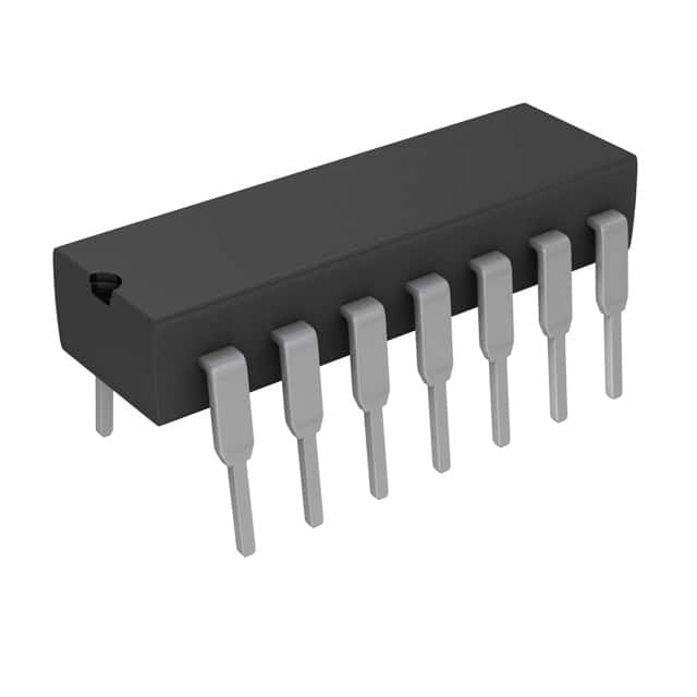
Xem thông số kỹ thuật để biết chi tiết sản phẩm.

SN74ACT04N
Product Overview
- Category: Integrated Circuit
- Use: Inverter
- Characteristics: High-speed, low-power consumption
- Package: DIP (Dual Inline Package)
- Essence: Hex inverter gate
- Packaging/Quantity: Tube/25 pieces
Specifications
- Supply Voltage Range: 4.5V to 5.5V
- Input Voltage Range: 0V to VCC
- Output Voltage Range: 0V to VCC
- Operating Temperature Range: -40°C to +85°C
- Propagation Delay Time: 6 ns (typical)
Detailed Pin Configuration
The SN74ACT04N has a total of 14 pins, numbered as follows:
- A1 (Input)
- Y1 (Output)
- A2 (Input)
- Y2 (Output)
- A3 (Input)
- Y3 (Output)
- GND (Ground)
- Y4 (Output)
- A4 (Input)
- Y5 (Output)
- A5 (Input)
- Y6 (Output)
- VCC (Power Supply)
- NC (No Connection)
Functional Features
- Hex Inverter: The SN74ACT04N consists of six independent inverters, each capable of converting a high-level input signal into its complementary low-level output.
- High-Speed Operation: With a propagation delay time of only 6 ns, this IC ensures fast signal processing.
- Low Power Consumption: The SN74ACT04N is designed to operate with low power consumption, making it suitable for battery-powered devices.
Advantages and Disadvantages
Advantages: - High-speed operation allows for quick signal processing. - Low power consumption makes it suitable for portable devices. - Hex inverter configuration provides flexibility in various applications.
Disadvantages: - Limited voltage range (4.5V to 5.5V) may not be compatible with all systems. - DIP package may require additional space compared to surface-mount packages.
Working Principles
The SN74ACT04N operates based on the principles of digital logic. Each inverter within the IC consists of transistors that control the flow of current, allowing it to invert the input signal and produce the complementary output.
Detailed Application Field Plans
The SN74ACT04N is widely used in various applications, including but not limited to: - Digital electronics - Microcontrollers - Communication systems - Signal processing - Industrial automation
Detailed and Complete Alternative Models
Some alternative models to the SN74ACT04N include: - CD4049UB: Hex Inverting Buffer/Converter - MC74ACT04: Hex Inverter - 74HC04: Hex Inverter
These alternatives offer similar functionality and can be used as replacements depending on specific requirements.
In conclusion, the SN74ACT04N is a high-speed, low-power hex inverter gate integrated circuit. Its compact DIP package and versatile functionality make it suitable for various digital applications. With its fast signal processing and low power consumption, it provides an efficient solution for many electronic systems.
Liệt kê 10 câu hỏi và câu trả lời thường gặp liên quan đến ứng dụng SN74ACT04N trong giải pháp kỹ thuật
Sure! Here are 10 common questions and answers related to the application of SN74ACT04N in technical solutions:
Q: What is SN74ACT04N? A: SN74ACT04N is a hex inverter gate IC (integrated circuit) that provides six independent inverters in a single package.
Q: What is the purpose of an inverter gate? A: An inverter gate is used to convert a logic level from one state to its opposite state. It takes an input signal and produces an output signal that is the logical complement of the input.
Q: What is the voltage supply range for SN74ACT04N? A: SN74ACT04N operates with a voltage supply range of 4.5V to 5.5V.
Q: What is the maximum operating frequency of SN74ACT04N? A: The maximum operating frequency of SN74ACT04N is typically around 100 MHz.
Q: Can SN74ACT04N be used with both TTL (Transistor-Transistor Logic) and CMOS (Complementary Metal-Oxide-Semiconductor) inputs? A: Yes, SN74ACT04N is compatible with both TTL and CMOS inputs.
Q: What is the output drive capability of SN74ACT04N? A: SN74ACT04N has a typical output drive capability of ±24 mA.
Q: Can SN74ACT04N be used as a level shifter? A: Yes, SN74ACT04N can be used as a level shifter to convert signals between different voltage levels.
Q: Is SN74ACT04N suitable for high-speed applications? A: Yes, SN74ACT04N is designed for high-speed operation and can be used in various high-speed digital applications.
Q: Can SN74ACT04N be used in both commercial and industrial environments? A: Yes, SN74ACT04N is suitable for use in both commercial and industrial environments.
Q: Are there any specific precautions to consider when using SN74ACT04N? A: It is important to ensure proper decoupling capacitors are used near the power supply pins of SN74ACT04N to minimize noise and voltage fluctuations. Additionally, care should be taken to avoid exceeding the maximum ratings specified in the datasheet, such as voltage and temperature limits.
Please note that these answers are general and may vary depending on the specific application and requirements. Always refer to the datasheet and consult with technical experts for accurate information.

