

Xem thông số kỹ thuật để biết chi tiết sản phẩm.
SN74AHC367DGVRG4
Product Overview
- Category: Integrated Circuit
- Use: Logic Level Shifter
- Characteristics: High-Speed, Low-Power, Non-Inverting
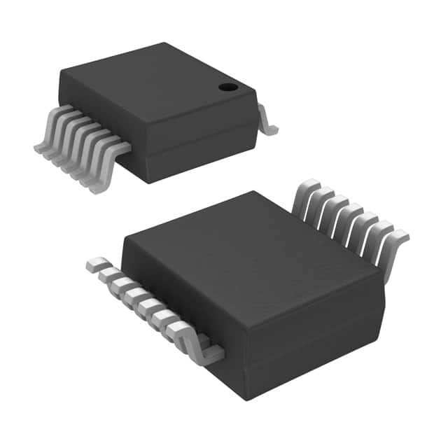
- Package: VSSOP-16
- Essence: Logic Level Translation
- Packaging/Quantity: Tape and Reel, 2500 pieces per reel
Specifications
The SN74AHC367DGVRG4 is an integrated circuit designed for logic level shifting applications. It operates at high speeds while consuming low power, making it suitable for various electronic devices. The device comes in a VSSOP-16 package, which provides compactness and ease of integration into circuit boards. Each reel contains 2500 pieces of the SN74AHC367DGVRG4.
Detailed Pin Configuration
The SN74AHC367DGVRG4 has a total of 16 pins, each serving a specific function. The pin configuration is as follows:
- OE (Output Enable)
- A1 (Input A1)
- B1 (Input B1)
- Y1 (Output Y1)
- GND (Ground)
- Y2 (Output Y2)
- B2 (Input B2)
- A2 (Input A2)
- OE (Output Enable)
- Y3 (Output Y3)
- GND (Ground)
- Y4 (Output Y4)
- B3 (Input B3)
- A3 (Input A3)
- OE (Output Enable)
- VCC (Power Supply)
Functional Features
The SN74AHC367DGVRG4 is primarily used for logic level translation between different voltage levels. It can convert signals from one logic family to another, allowing seamless communication between devices operating at different voltage levels. The device offers non-inverting functionality, ensuring that the output signal maintains the same logic state as the input signal.
Advantages and Disadvantages
Advantages: - High-speed operation - Low power consumption - Non-inverting functionality - Compact VSSOP-16 package for easy integration
Disadvantages: - Limited voltage translation range - Not suitable for bidirectional level shifting
Working Principles
The SN74AHC367DGVRG4 utilizes a combination of MOSFETs and CMOS technology to achieve logic level translation. When an input signal is applied, the device detects the logic state and translates it to the corresponding output voltage level. The non-inverting feature ensures that the output signal matches the input signal's logic state.
Detailed Application Field Plans
The SN74AHC367DGVRG4 finds applications in various electronic devices where logic level translation is required. Some potential application fields include:
- Microcontrollers: The device can be used to interface microcontrollers operating at different voltage levels.
- Communication Systems: It enables communication between devices with varying logic voltage levels, such as UART or SPI interfaces.
- Sensor Networks: The SN74AHC367DGVRG4 facilitates data exchange between sensors and microcontrollers with different voltage requirements.
- Industrial Automation: It can be utilized in control systems to interface different logic families used in industrial automation equipment.
Detailed and Complete Alternative Models
- SN74LVC1T45DBVR: Single-Bit Dual-Supply Bus Transceiver
- SN74LVCH245ADBR: Octal Bus Transceiver with 3-State Outputs
- SN74HCT125N: Quadruple Bus Buffer Gates with 3-State Outputs
- SN74LVC8T245PWR: 8-Bit Dual-Supply Bus Transceiver with Configurable Voltage Translation
These alternative models offer similar functionality to the SN74AHC367DGVRG4 and can be considered as alternatives based on specific requirements.
Word count: 408 words
Liệt kê 10 câu hỏi và câu trả lời thường gặp liên quan đến ứng dụng SN74AHC367DGVRG4 trong giải pháp kỹ thuật
What is the maximum operating voltage for SN74AHC367DGVRG4?
- The maximum operating voltage for SN74AHC367DGVRG4 is 5.5V.What is the typical input capacitance of SN74AHC367DGVRG4?
- The typical input capacitance of SN74AHC367DGVRG4 is 3.5pF.Can SN74AHC367DGVRG4 be used in automotive applications?
- Yes, SN74AHC367DGVRG4 is suitable for use in automotive applications.What is the output drive capability of SN74AHC367DGVRG4?
- SN74AHC367DGVRG4 has a high output drive capability, making it suitable for driving heavy loads.Is SN74AHC367DGVRG4 compatible with both CMOS and TTL inputs?
- Yes, SN74AHC367DGVRG4 is compatible with both CMOS and TTL inputs.What is the maximum propagation delay of SN74AHC367DGVRG4?
- The maximum propagation delay of SN74AHC367DGVRG4 is 8ns.Can SN74AHC367DGVRG4 be used in battery-powered devices?
- Yes, SN74AHC367DGVRG4 is suitable for use in battery-powered devices due to its low power consumption.Does SN74AHC367DGVRG4 have built-in ESD protection?
- Yes, SN74AHC367DGVRG4 features built-in ESD protection for enhanced reliability.What is the temperature range for SN74AHC367DGVRG4?
- SN74AHC367DGVRG4 operates within a temperature range of -40°C to 125°C.Is SN74AHC367DGVRG4 available in a small form factor package?
- Yes, SN74AHC367DGVRG4 is available in a small and space-saving VSSOP package.