

Xem thông số kỹ thuật để biết chi tiết sản phẩm.
SN74ALVC126DGVRE4
Product Overview
Category
SN74ALVC126DGVRE4 belongs to the category of integrated circuits (ICs).
Use
This IC is commonly used as a quad buffer/line driver with 3-state outputs.
Characteristics
- High-speed CMOS technology
- Low power consumption
- 3.3V voltage supply
- 3-state outputs for bus-oriented applications
- Schmitt-trigger inputs for noise immunity
- Available in various package options
Package
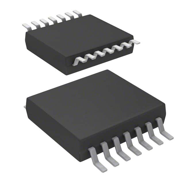
SN74ALVC126DGVRE4 is available in a small-sized, surface-mount package.
Essence
The essence of SN74ALVC126DGVRE4 lies in its ability to provide buffering and line driving functions for digital signals in electronic circuits.
Packaging/Quantity
This IC is typically packaged in reels or tubes, with a quantity of 2500 units per reel/tube.
Specifications
- Supply Voltage: 2.7V to 3.6V
- Input Voltage Range: 0V to VCC
- Output Voltage Range: 0V to VCC
- Operating Temperature Range: -40°C to +85°C
- Propagation Delay Time: 3.5ns (typical)
- Output Current: ±24mA
Detailed Pin Configuration
SN74ALVC126DGVRE4 has a total of 14 pins, which are assigned specific functions as follows:
- Pin 1: Output Enable (OE) for Buffer 1
- Pin 2: Input (A) for Buffer 1
- Pin 3: Output (Y) for Buffer 1
- Pin 4: Ground (GND)
- Pin 5: Output (Y) for Buffer 2
- Pin 6: Input (B) for Buffer 2
- Pin 7: Output Enable (OE) for Buffer 2
- Pin 8: VCC (Positive Power Supply)
- Pin 9: Input (C) for Buffer 3
- Pin 10: Output (Y) for Buffer 3
- Pin 11: Output Enable (OE) for Buffer 3
- Pin 12: Input (D) for Buffer 4
- Pin 13: Output (Y) for Buffer 4
- Pin 14: VCC (Positive Power Supply)
Functional Features
- Quad buffer/line driver with 3-state outputs
- Allows bidirectional flow of data
- Provides buffering and line driving functions
- Schmitt-trigger inputs for improved noise immunity
- High-speed operation suitable for bus-oriented applications
Advantages and Disadvantages
Advantages
- Low power consumption
- High-speed CMOS technology
- Noise-immune Schmitt-trigger inputs
- 3-state outputs for bus-oriented applications
Disadvantages
- Limited voltage supply range (2.7V to 3.6V)
- Not suitable for high-voltage applications
Working Principles
SN74ALVC126DGVRE4 operates by receiving digital input signals through its four input pins (A, B, C, D). These signals are then buffered and amplified by the internal circuitry. The output signals (Y) can be enabled or disabled using the respective output enable pins (OE). The 3-state outputs allow multiple devices to share a common bus without interfering with each other.
Detailed Application Field Plans
SN74ALVC126DGVRE4 finds applications in various fields, including:
- Microcontrollers and microprocessors
- Data communication systems
- Industrial automation
- Automotive electronics
- Consumer electronics
Detailed and Complete Alternative Models
- SN74ALVC126DGVRE4
- SN74LVC126ADGVR
- MC74VHC126DTG
- 74LVCH126APW,118
- CD74HCT126M96
These alternative models offer similar functionality and can be used as substitutes for SN74ALVC126DGVRE4 in different applications.
Word count: 450 words
Liệt kê 10 câu hỏi và câu trả lời thường gặp liên quan đến ứng dụng SN74ALVC126DGVRE4 trong giải pháp kỹ thuật
Sure! Here are 10 common questions and answers related to the application of SN74ALVC126DGVRE4 in technical solutions:
Q: What is SN74ALVC126DGVRE4? A: SN74ALVC126DGVRE4 is a quad buffer/line driver with 3-state outputs, commonly used in digital logic applications.
Q: What is the operating voltage range for SN74ALVC126DGVRE4? A: The operating voltage range for SN74ALVC126DGVRE4 is typically between 1.65V and 3.6V.
Q: What is the maximum output current that SN74ALVC126DGVRE4 can drive? A: SN74ALVC126DGVRE4 can drive up to 24mA of output current per channel.
Q: Can SN74ALVC126DGVRE4 be used as a level shifter? A: Yes, SN74ALVC126DGVRE4 can be used as a level shifter to convert signals between different voltage levels.
Q: How many channels does SN74ALVC126DGVRE4 have? A: SN74ALVC126DGVRE4 has four independent channels, each with a separate input and output.
Q: What is the propagation delay of SN74ALVC126DGVRE4? A: The typical propagation delay of SN74ALVC126DGVRE4 is around 3.8ns.
Q: Can SN74ALVC126DGVRE4 be used in high-speed applications? A: Yes, SN74ALVC126DGVRE4 is designed for high-speed operation and can be used in applications with fast switching requirements.
Q: Does SN74ALVC126DGVRE4 have built-in ESD protection? A: Yes, SN74ALVC126DGVRE4 has built-in ESD protection to safeguard against electrostatic discharge.
Q: Can SN74ALVC126DGVRE4 be used in both input and output buffer applications? A: Yes, SN74ALVC126DGVRE4 can be used as both an input buffer and an output buffer, depending on the application requirements.
Q: Is SN74ALVC126DGVRE4 RoHS compliant? A: Yes, SN74ALVC126DGVRE4 is RoHS compliant, meaning it meets the Restriction of Hazardous Substances directive.
Please note that these answers are general and may vary based on specific datasheet specifications or application requirements.