

Xem thông số kỹ thuật để biết chi tiết sản phẩm.
SN74AUC17RGYRG4
Product Overview
- Category: Integrated Circuit (IC)
- Use: Logic Gate
- Characteristics: High-speed, low-power, Schmitt-trigger input
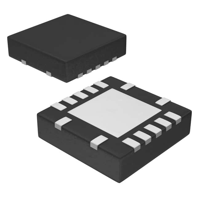
- Package: VQFN (Very Thin Quad Flat No-Lead)
- Essence: Triple Schmitt-trigger buffer
- Packaging/Quantity: Tape and Reel, 2500 units per reel
Specifications
- Supply Voltage Range: 0.8V to 3.6V
- Input Voltage Range: -0.5V to 4.6V
- Output Voltage Range: 0V to VCC
- Operating Temperature Range: -40°C to +85°C
- Propagation Delay: 2.1ns (typical)
- Maximum Quiescent Current: 10μA
Detailed Pin Configuration
The SN74AUC17RGYRG4 has a total of 14 pins, which are labeled as follows:
- A1: Input A1
- Y1: Output Y1
- A2: Input A2
- Y2: Output Y2
- GND: Ground
- A3: Input A3
- Y3: Output Y3
- VCC: Power Supply
- NC: Not Connected
- NC: Not Connected
- NC: Not Connected
- NC: Not Connected
- NC: Not Connected
- NC: Not Connected
Functional Features
- Triple Schmitt-trigger buffers with open-drain outputs
- Wide supply voltage range allows compatibility with various systems
- Low power consumption makes it suitable for battery-powered devices
- Schmitt-trigger inputs provide hysteresis for noise immunity
- Open-drain outputs allow easy interfacing with other devices
Advantages and Disadvantages
Advantages: - High-speed operation - Low power consumption - Wide supply voltage range - Schmitt-trigger inputs for noise immunity - Open-drain outputs for easy interfacing
Disadvantages: - Limited number of buffer gates (3 in this case) - Not suitable for applications requiring a large number of logic gates
Working Principles
The SN74AUC17RGYRG4 is a triple Schmitt-trigger buffer IC. It operates by amplifying and shaping input signals to provide clean and stable output signals. The Schmitt-trigger inputs ensure that the output transitions occur at well-defined voltage levels, making the IC less susceptible to noise and signal fluctuations. The open-drain outputs allow multiple devices to be connected together, enabling wired-OR configurations.
Detailed Application Field Plans
The SN74AUC17RGYRG4 can be used in various applications, including but not limited to:
- Digital communication systems
- Microcontroller-based projects
- Sensor interfaces
- Signal conditioning circuits
- Battery-powered devices
- Industrial automation systems
- Automotive electronics
- Consumer electronics
Detailed and Complete Alternative Models
- SN74AUC14RGYRG4: Hex Schmitt-trigger inverter
- SN74AUC32RGYRG4: Quad 2-input Schmitt-trigger OR gate
- SN74AUC125RGYRG4: Quad 3-state non-inverting buffer
These alternative models offer similar functionality and characteristics, providing flexibility in choosing the appropriate IC for specific applications.
Word count: 408 words
Liệt kê 10 câu hỏi và câu trả lời thường gặp liên quan đến ứng dụng SN74AUC17RGYRG4 trong giải pháp kỹ thuật
Sure! Here are 10 common questions and answers related to the application of SN74AUC17RGYRG4 in technical solutions:
Q: What is SN74AUC17RGYRG4? A: SN74AUC17RGYRG4 is a triple Schmitt-trigger buffer/driver integrated circuit (IC) that can be used for signal conditioning and level shifting applications.
Q: What is the operating voltage range of SN74AUC17RGYRG4? A: The operating voltage range of SN74AUC17RGYRG4 is from 0.8V to 3.6V.
Q: How many Schmitt-trigger buffers/drivers are there in SN74AUC17RGYRG4? A: SN74AUC17RGYRG4 consists of three independent Schmitt-trigger buffers/drivers.
Q: What is the maximum output current of SN74AUC17RGYRG4? A: The maximum output current of SN74AUC17RGYRG4 is typically 24mA.
Q: Can SN74AUC17RGYRG4 be used for level shifting between different voltage domains? A: Yes, SN74AUC17RGYRG4 can be used for level shifting between different voltage domains due to its wide operating voltage range.
Q: What is the propagation delay of SN74AUC17RGYRG4? A: The propagation delay of SN74AUC17RGYRG4 is typically around 2.7ns.
Q: Is SN74AUC17RGYRG4 suitable for high-speed applications? A: Yes, SN74AUC17RGYRG4 is designed for high-speed operation and can be used in applications with fast switching requirements.
Q: Can SN74AUC17RGYRG4 be used for bidirectional signal buffering? A: No, SN74AUC17RGYRG4 is a unidirectional buffer/driver and does not support bidirectional signal buffering.
Q: What is the package type of SN74AUC17RGYRG4? A: SN74AUC17RGYRG4 is available in a 14-pin VQFN (Very Thin Quad Flat No-Lead) package.
Q: Are there any special considerations for using SN74AUC17RGYRG4 in noisy environments? A: Yes, it is recommended to use proper decoupling capacitors near the power supply pins of SN74AUC17RGYRG4 to minimize noise interference.
Please note that these answers are general and may vary depending on specific application requirements. It is always advisable to refer to the datasheet and consult the manufacturer for detailed information.