

Xem thông số kỹ thuật để biết chi tiết sản phẩm.
SN74AUC2G34YEPR
Product Overview
- Category: Integrated Circuit (IC)
- Use: Logic Gate
- Characteristics: Dual Buffer/Driver, Non-Inverting, 2-Input, 1-Output
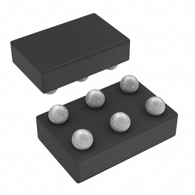
- Package: 8-Pin DSBGA (MicroStar Junior™), Tape and Reel
- Essence: High-Speed CMOS Logic
- Packaging/Quantity: 3000 units per reel
Specifications
- Supply Voltage Range: 0.8V to 3.6V
- Input Voltage Range: 0V to VCC
- Output Voltage Range: 0V to VCC
- High-Level Input Voltage: 0.7VCC to VCC
- Low-Level Input Voltage: 0V to 0.3VCC
- High-Level Output Voltage: 0.9VCC to VCC
- Low-Level Output Voltage: 0V to 0.1VCC
- Maximum Operating Frequency: 500MHz
- Propagation Delay: 2.5ns (typical)
Detailed Pin Configuration
The SN74AUC2G34YEPR has the following pin configuration:
```
| | --| A | --| B Y | --| GND GND | --| Y B | --| A | --| VCC VCC | |___________| ```
Functional Features
- Dual buffer/driver with non-inverting logic.
- Provides signal amplification and level shifting.
- Supports high-speed data transmission.
- Wide operating voltage range allows compatibility with various systems.
- Low power consumption.
Advantages and Disadvantages
Advantages: - High-speed operation enables efficient data processing. - Compact package size saves board space. - Wide supply voltage range enhances versatility. - Low power consumption reduces energy requirements.
Disadvantages: - Limited number of inputs and outputs. - Not suitable for applications requiring complex logic functions. - Sensitivity to electrostatic discharge (ESD) requires proper handling precautions.
Working Principles
The SN74AUC2G34YEPR is based on high-speed CMOS technology. It consists of two buffer/driver circuits that amplify and transmit input signals to the output pin. The non-inverting nature of the device ensures that the output signal matches the input signal polarity. The IC operates within a wide supply voltage range, allowing it to interface with various logic families and systems.
Detailed Application Field Plans
The SN74AUC2G34YEPR is commonly used in the following applications:
- Communication Systems: Provides signal buffering and level shifting in high-speed data transmission interfaces.
- Consumer Electronics: Enables voltage level conversion between different components in portable devices.
- Industrial Automation: Facilitates signal amplification and interfacing in control systems.
- Automotive Electronics: Supports data communication and signal conditioning in automotive modules.
- Medical Devices: Ensures reliable signal transmission and compatibility in medical equipment.
Detailed and Complete Alternative Models
- SN74AUC2G34YZPR: Similar specifications and features, but available in a different package (8-Pin X2SON).
- SN74LVC2G34DBVR: Dual buffer/driver with similar functionality, but operates at a higher voltage range (1.65V to 5.5V).
- SN74HC2G34QDCKR: Non-inverting buffer/driver with comparable performance, but designed for operation at a lower frequency range (up to 50MHz).
(Note: This list is not exhaustive and other alternative models may exist.)
Word count: 366 words
Liệt kê 10 câu hỏi và câu trả lời thường gặp liên quan đến ứng dụng SN74AUC2G34YEPR trong giải pháp kỹ thuật
Sure! Here are 10 common questions and answers related to the application of SN74AUC2G34YEPR in technical solutions:
Q: What is the SN74AUC2G34YEPR? A: The SN74AUC2G34YEPR is a dual buffer gate IC (integrated circuit) that provides high-speed signal buffering and voltage level shifting capabilities.
Q: What is the operating voltage range of SN74AUC2G34YEPR? A: The SN74AUC2G34YEPR operates within a voltage range of 0.8V to 3.6V.
Q: What is the maximum data rate supported by SN74AUC2G34YEPR? A: The SN74AUC2G34YEPR supports a maximum data rate of 500 Mbps (megabits per second).
Q: Can SN74AUC2G34YEPR be used for bidirectional signal buffering? A: No, the SN74AUC2G34YEPR is a unidirectional buffer and cannot be used for bidirectional signal buffering.
Q: What is the output drive strength of SN74AUC2G34YEPR? A: The SN74AUC2G34YEPR has a typical output drive strength of ±24 mA.
Q: Is SN74AUC2G34YEPR suitable for level shifting between different voltage domains? A: Yes, SN74AUC2G34YEPR can be used for level shifting between voltage domains due to its wide operating voltage range.
Q: Can SN74AUC2G34YEPR tolerate overvoltage or undervoltage conditions? A: No, SN74AUC2G34YEPR is not designed to tolerate overvoltage or undervoltage conditions. It should be operated within the specified voltage range.
Q: What is the package type of SN74AUC2G34YEPR? A: SN74AUC2G34YEPR is available in a small SOT-553 package.
Q: Can SN74AUC2G34YEPR be used in high-speed digital communication applications? A: Yes, SN74AUC2G34YEPR is suitable for high-speed digital communication applications such as data transmission and clock distribution.
Q: Are there any recommended external components required for using SN74AUC2G34YEPR? A: No, SN74AUC2G34YEPR does not require any external components for its basic operation. However, decoupling capacitors may be recommended for noise reduction in certain applications.
Please note that these answers are general and it's always important to refer to the datasheet and consult with the manufacturer for specific application requirements and guidelines.