

Xem thông số kỹ thuật để biết chi tiết sản phẩm.
SN74AUP1G08DRYR
Product Overview
- Category: Integrated Circuit (IC)
- Use: Logic Gate
- Characteristics: Single 2-input AND gate
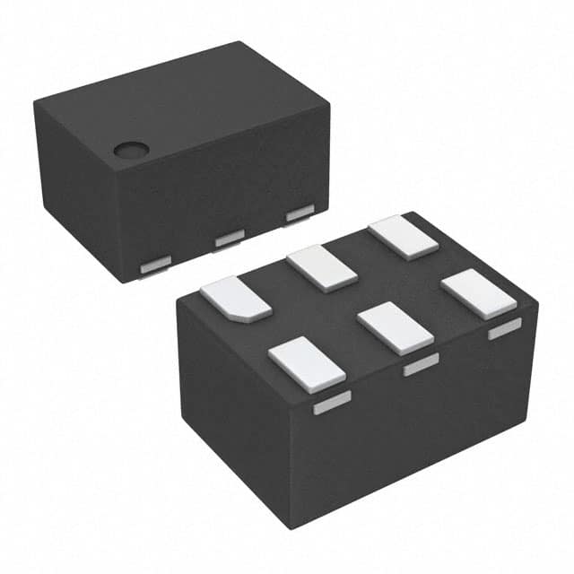
- Package: SOT-23-5
- Essence: High-performance CMOS technology
- Packaging/Quantity: Tape and Reel, 3000 units per reel
Specifications
- Supply Voltage Range: 0.8V to 3.6V
- Input Voltage Range: -0.5V to VCC + 0.5V
- Output Voltage Range: 0V to VCC
- Operating Temperature Range: -40°C to 125°C
- Propagation Delay: 2.9ns (typical)
- Maximum Quiescent Current: 10μA
- Maximum Output Current: ±8mA
Detailed Pin Configuration
The SN74AUP1G08DRYR has a total of 5 pins:
- GND (Ground): Connected to the ground reference potential.
- A (Input A): First input terminal for the AND gate.
- B (Input B): Second input terminal for the AND gate.
- Y (Output): Output terminal of the AND gate.
- VCC (Supply Voltage): Connected to the positive supply voltage.
Functional Features
- High-speed operation: The SN74AUP1G08DRYR utilizes high-performance CMOS technology, allowing for fast logic operations.
- Low power consumption: With a maximum quiescent current of only 10μA, this IC is designed to be energy-efficient.
- Wide operating voltage range: The supply voltage can range from 0.8V to 3.6V, providing flexibility in various applications.
- Small package size: The SOT-23-5 package offers compactness and ease of integration into electronic circuits.
Advantages and Disadvantages
Advantages: - High-speed operation enables quick response times. - Low power consumption prolongs battery life in portable devices. - Wide operating voltage range allows compatibility with different power sources. - Small package size saves space on circuit boards.
Disadvantages: - Limited number of inputs (only 2) restricts complex logic operations. - Sensitive to electrostatic discharge (ESD), requiring proper handling during assembly.
Working Principles
The SN74AUP1G08DRYR is a single 2-input AND gate. It performs the logical AND operation on its two input signals, A and B, and produces the corresponding output signal, Y. The gate operates based on CMOS technology, utilizing MOSFET transistors to control the flow of current through the circuit. When both input signals are high (logic level 1), the output signal will also be high. Otherwise, the output signal will be low (logic level 0).
Detailed Application Field Plans
The SN74AUP1G08DRYR can be used in various applications, including but not limited to:
- Digital Logic Circuits: The AND gate is a fundamental building block in digital systems, used for combining multiple input signals to generate desired output signals.
- Microcontrollers and Microprocessors: This IC can be employed in the input/output (I/O) interface circuitry of microcontrollers and microprocessors to perform logical operations.
- Communication Systems: The AND gate is utilized in communication systems for signal processing, data encoding, and decoding.
- Industrial Automation: The IC can be integrated into industrial automation systems for controlling and monitoring processes.
Detailed and Complete Alternative Models
- SN74AUP1G00DCKR: Single 2-input NAND gate, SOT-23-5 package.
- SN74AUP1G02DCKR: Single 2-input NOR gate, SOT-23-5 package.
- SN74AUP1G04DCKR: Single inverter (NOT gate), SOT-23-5 package.
- SN74AUP1G32DCKR: Single 2-input OR gate, SOT-23-5 package.
These alternative models offer similar functionality to the SN74AUP1G08DRYR but with different logical operations.
Word count: 531 words
Liệt kê 10 câu hỏi và câu trả lời thường gặp liên quan đến ứng dụng SN74AUP1G08DRYR trong giải pháp kỹ thuật
Sure! Here are 10 common questions and answers related to the application of SN74AUP1G08DRYR in technical solutions:
1. What is SN74AUP1G08DRYR? SN74AUP1G08DRYR is a single 2-input AND gate IC (integrated circuit) that operates at a voltage range of 0.8V to 3.6V.
2. What is the purpose of SN74AUP1G08DRYR? The purpose of SN74AUP1G08DRYR is to perform logical AND operations on two input signals, producing an output signal based on their logical states.
3. What are the key features of SN74AUP1G08DRYR? Some key features of SN74AUP1G08DRYR include low power consumption, wide operating voltage range, high-speed operation, and compatibility with various logic families.
4. What are the typical applications of SN74AUP1G08DRYR? SN74AUP1G08DRYR is commonly used in applications such as data communication systems, portable devices, battery-powered systems, and general-purpose logic circuits.
5. What is the maximum operating frequency of SN74AUP1G08DRYR? The maximum operating frequency of SN74AUP1G08DRYR is typically around 500 MHz.
6. Can SN74AUP1G08DRYR be used with other logic families? Yes, SN74AUP1G08DRYR is compatible with various logic families such as CMOS, TTL, and LVCMOS.
7. What is the input voltage threshold for SN74AUP1G08DRYR? The input voltage threshold for SN74AUP1G08DRYR is typically around 0.8V.
8. What is the output voltage level of SN74AUP1G08DRYR? The output voltage level of SN74AUP1G08DRYR is typically equal to the supply voltage (VCC).
9. Can SN74AUP1G08DRYR be used in high-temperature environments? SN74AUP1G08DRYR has a maximum operating temperature of 125°C, making it suitable for use in moderately high-temperature environments.
10. Is SN74AUP1G08DRYR available in different package options? Yes, SN74AUP1G08DRYR is available in various package options such as SOT-23, X2SON, and DCK packages, providing flexibility for different application requirements.
Please note that the answers provided here are general and may vary depending on specific datasheet specifications and application considerations.