

Xem thông số kỹ thuật để biết chi tiết sản phẩm.
SN74AUP2G240RSER
Product Overview
- Category: Integrated Circuit
- Use: Logic Gate
- Characteristics: Dual Buffer/Driver
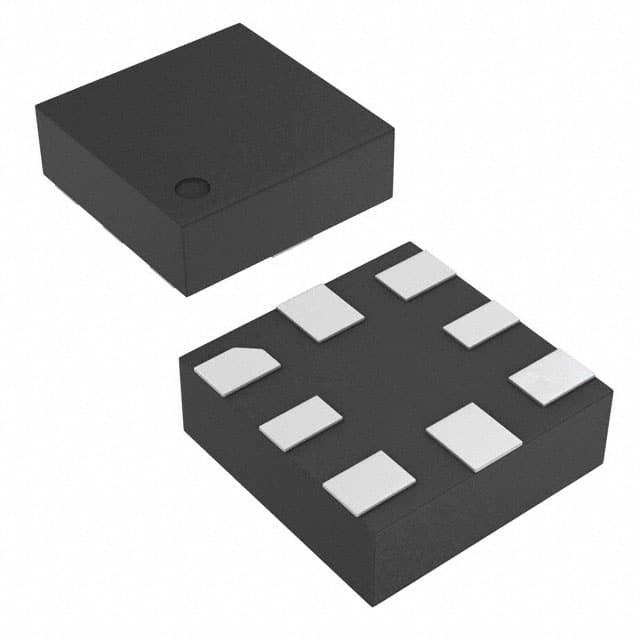
- Package: Small Outline Package (SOP)
- Essence: High-Speed CMOS Technology
- Packaging/Quantity: Tape and Reel, 3000 pieces per reel
Specifications
- Supply Voltage Range: 0.8V to 3.6V
- Input Voltage Range: -0.5V to VCC + 0.5V
- Output Voltage Range: 0V to VCC
- Maximum Operating Frequency: 500MHz
- Propagation Delay: 1.9ns (typical)
- Output Drive Capability: ±24mA
- ESD Protection: Human Body Model > 2000V
Detailed Pin Configuration
The SN74AUP2G240RSER has a total of 8 pins:
- GND (Ground)
- A Input 1
- Y Output 1
- B Input 2
- Y Output 2
- OE (Output Enable)
- VCC (Supply Voltage)
- GND (Ground)
Functional Features
- Dual buffer/driver with independent control for each channel
- High-speed operation suitable for various applications
- Wide supply voltage range allows compatibility with different systems
- Low power consumption
- ESD protection for enhanced reliability
Advantages and Disadvantages
Advantages: - Dual-channel design provides flexibility in signal routing - High-speed operation enables efficient data transmission - Wide supply voltage range allows compatibility with various systems - Low power consumption helps conserve energy - ESD protection enhances the reliability of the device
Disadvantages: - Limited output drive capability compared to some other models - Not suitable for high-power applications
Working Principles
The SN74AUP2G240RSER is a dual buffer/driver integrated circuit that operates using high-speed CMOS technology. It consists of two independent channels, each with an input and output. The device can be controlled using the OE (Output Enable) pin, which allows for individual channel activation.
When the OE pin is low, the inputs are buffered and transferred to the outputs. Conversely, when the OE pin is high, the outputs are in a high-impedance state, effectively disconnecting them from the inputs.
The device operates within a wide supply voltage range, allowing it to be used in various systems. It also features ESD protection, which safeguards against electrostatic discharge and enhances its reliability.
Detailed Application Field Plans
The SN74AUP2G240RSER is commonly used in applications that require signal buffering or driving. Some specific application fields include:
- Communication Systems: The device can be used to buffer or drive signals in communication systems such as routers, switches, and modems.
- Consumer Electronics: It finds applications in consumer electronic devices like smartphones, tablets, and gaming consoles, where it helps in signal routing and amplification.
- Industrial Automation: The SN74AUP2G240RSER is suitable for industrial automation systems, providing signal buffering and driving capabilities in control panels, PLCs, and motor drives.
- Automotive Electronics: It can be utilized in automotive electronics for signal conditioning, level shifting, and driving applications.
Detailed and Complete Alternative Models
- SN74AUP2G241RSER: Similar to SN74AUP2G240RSER but with inverted outputs.
- SN74LVC2G240RSER: Dual buffer/driver with lower power consumption and higher output drive capability.
- SN74LV2G07RSER: Dual buffer/driver with open-drain outputs for wired-OR applications.
- SN74AUP1G240RSER: Single-channel buffer/driver with similar characteristics and package.
These alternative models offer different features and specifications, allowing users to choose the most suitable option for their specific requirements.
Word count: 523 words
Liệt kê 10 câu hỏi và câu trả lời thường gặp liên quan đến ứng dụng SN74AUP2G240RSER trong giải pháp kỹ thuật
Sure! Here are 10 common questions and answers related to the application of SN74AUP2G240RSER in technical solutions:
Q: What is SN74AUP2G240RSER? A: SN74AUP2G240RSER is a dual buffer/line driver IC (integrated circuit) designed for voltage level translation applications.
Q: What is the voltage range supported by SN74AUP2G240RSER? A: SN74AUP2G240RSER supports voltage translation from 0.8V to 3.6V, making it suitable for various low-voltage applications.
Q: Can SN74AUP2G240RSER be used as a bidirectional level shifter? A: No, SN74AUP2G240RSER is a unidirectional buffer/line driver and does not support bidirectional level shifting.
Q: What is the maximum data rate supported by SN74AUP2G240RSER? A: SN74AUP2G240RSER can handle data rates up to 100 MHz, making it suitable for high-speed applications.
Q: How many input/output pins does SN74AUP2G240RSER have? A: SN74AUP2G240RSER has two input pins and two output pins, allowing for translation between two different voltage domains.
Q: Can SN74AUP2G240RSER be used with both CMOS and TTL logic levels? A: Yes, SN74AUP2G240RSER is compatible with both CMOS and TTL logic levels, providing flexibility in various system designs.
Q: Does SN74AUP2G240RSER have built-in ESD protection? A: Yes, SN74AUP2G240RSER has built-in ESD (electrostatic discharge) protection, ensuring robustness against electrostatic events.
Q: What is the power supply voltage range for SN74AUP2G240RSER? A: SN74AUP2G240RSER operates with a power supply voltage range of 0.8V to 3.6V, making it compatible with various power sources.
Q: Can SN74AUP2G240RSER be used in battery-powered applications? A: Yes, SN74AUP2G240RSER's low power consumption and wide operating voltage range make it suitable for battery-powered devices.
Q: Are there any application notes or reference designs available for SN74AUP2G240RSER? A: Yes, Texas Instruments provides application notes and reference designs that can help users understand and implement SN74AUP2G240RSER in their technical solutions.
Please note that these answers are general and may vary depending on specific design requirements and use cases. It is always recommended to refer to the datasheet and consult with the manufacturer for detailed information.