

Xem thông số kỹ thuật để biết chi tiết sản phẩm.
SN74CBTLV3253RGYR
Product Overview
- Category: Integrated Circuit
- Use: Multiplexer/Demultiplexer
- Characteristics: Low voltage, high-speed switching, low power consumption
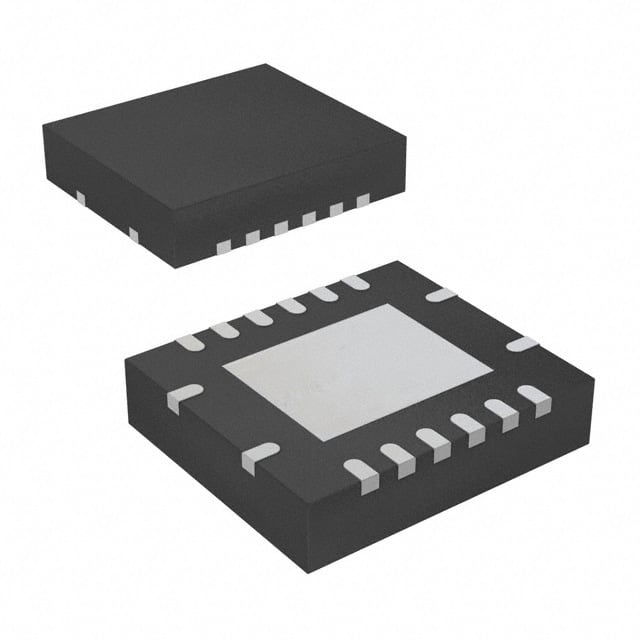
- Package: 16-VQFN (3.5mm x 3.5mm)
- Essence: A versatile multiplexer/demultiplexer IC designed for low voltage applications
- Packaging/Quantity: Tape and Reel, 2500 units per reel
Specifications
- Supply Voltage Range: 1.65V to 3.6V
- On-State Resistance: 4Ω (typical)
- Bandwidth: 400MHz (typical)
- Number of Channels: 2
- Input/Output Capacitance: 3pF (typical)
- Operating Temperature Range: -40°C to +85°C
Detailed Pin Configuration
The SN74CBTLV3253RGYR has a 16-pin VQFN package with the following pin configuration:
Pin 1: Channel 1 Select (S1)
Pin 2: Channel 2 Select (S2)
Pin 3: Ground (GND)
Pin 4: Channel 1 Data Input/Output (I/O1)
Pin 5: Channel 2 Data Input/Output (I/O2)
Pin 6: Channel 1 Enable (E1)
Pin 7: Channel 2 Enable (E2)
Pin 8: VCC
Pin 9: Channel 1 Output Enable (OE1)
Pin 10: Channel 2 Output Enable (OE2)
Pin 11: Channel 1 Inverted Output Enable (OE1')
Pin 12: Channel 2 Inverted Output Enable (OE2')
Pin 13: Channel 1 Inverted Output (O1')
Pin 14: Channel 2 Inverted Output (O2')
Pin 15: Channel 1 Output (O1)
Pin 16: Channel 2 Output (O2)
Functional Features
- Dual-channel multiplexer/demultiplexer functionality
- Low voltage operation suitable for battery-powered devices
- High-speed switching capability for efficient data transmission
- Low power consumption for energy-efficient applications
- Wide operating temperature range for versatile usage scenarios
Advantages and Disadvantages
Advantages: - Versatile multiplexer/demultiplexer IC suitable for various applications - Low voltage operation enables compatibility with a wide range of devices - High-speed switching allows for efficient data transfer - Low power consumption extends battery life in portable devices - Compact package size saves board space
Disadvantages: - Limited number of channels may not be sufficient for complex systems requiring more inputs/outputs - On-state resistance may introduce signal attenuation in high-frequency applications
Working Principles
The SN74CBTLV3253RGYR is designed to function as a dual-channel multiplexer/demultiplexer. It allows the selection of one of two input channels to be routed to the output channel based on the control signals provided. The device operates at low voltages, making it suitable for use in battery-powered devices.
Detailed Application Field Plans
The SN74CBTLV3253RGYR finds applications in various fields, including:
- Consumer Electronics: Used in audio/video equipment for signal routing and switching.
- Telecommunications: Enables efficient data transmission in communication systems.
- Automotive: Facilitates signal routing in automotive infotainment systems.
- Industrial Automation: Used in control systems for signal selection and distribution.
- Medical Devices: Enables signal routing in medical imaging and diagnostic equipment.
Detailed and Complete Alternative Models
- CD74HC4051E: 8-channel analog multiplexer/demultiplexer IC.
- SN74LVC1G3157DBVR: Single-channel analog switch with low voltage operation.
- ADG732BSUZ-REEL7: 16-channel digital multiplexer/demultiplexer IC.
These alternative models offer similar functionality and can be considered as alternatives to the SN74CBTLV3253RGYR based on specific application requirements.
Word count: 411 words
Liệt kê 10 câu hỏi và câu trả lời thường gặp liên quan đến ứng dụng SN74CBTLV3253RGYR trong giải pháp kỹ thuật
Sure! Here are 10 common questions and answers related to the application of SN74CBTLV3253RGYR:
Q: What is the SN74CBTLV3253RGYR? A: The SN74CBTLV3253RGYR is a dual 1-of-4 high-speed CMOS analog multiplexer/demultiplexer IC.
Q: What is the purpose of the SN74CBTLV3253RGYR? A: This IC is used for routing analog signals in various technical solutions, such as audio/video switching, data acquisition systems, and communication devices.
Q: What is the operating voltage range of the SN74CBTLV3253RGYR? A: The operating voltage range is typically between 1.65V and 5.5V.
Q: How many channels does the SN74CBTLV3253RGYR have? A: It has two independent channels, each with four multiplexers/demultiplexers.
Q: What is the maximum frequency at which the SN74CBTLV3253RGYR can operate? A: The maximum frequency is typically around 400 MHz.
Q: Can the SN74CBTLV3253RGYR handle both analog and digital signals? A: Yes, it can handle both analog and digital signals, making it versatile for different applications.
Q: Does the SN74CBTLV3253RGYR have built-in ESD protection? A: Yes, it has built-in ESD protection, which helps safeguard against electrostatic discharge.
Q: What is the package type of the SN74CBTLV3253RGYR? A: It comes in a small 16-pin VQFN package.
Q: Can the SN74CBTLV3253RGYR be used in battery-powered devices? A: Yes, it can be used in battery-powered devices due to its low power consumption characteristics.
Q: Are there any application notes or reference designs available for the SN74CBTLV3253RGYR? A: Yes, Texas Instruments provides application notes and reference designs that can help with the implementation of this IC in various technical solutions.
Please note that the answers provided here are general and may vary depending on specific datasheet specifications and application requirements.