

Xem thông số kỹ thuật để biết chi tiết sản phẩm.
SN74CBTLV3861DGVR
Product Overview
- Category: Integrated Circuit (IC)
- Use: Digital Multiplexer/Demultiplexer
- Characteristics: Low voltage, high-speed switching, low power consumption
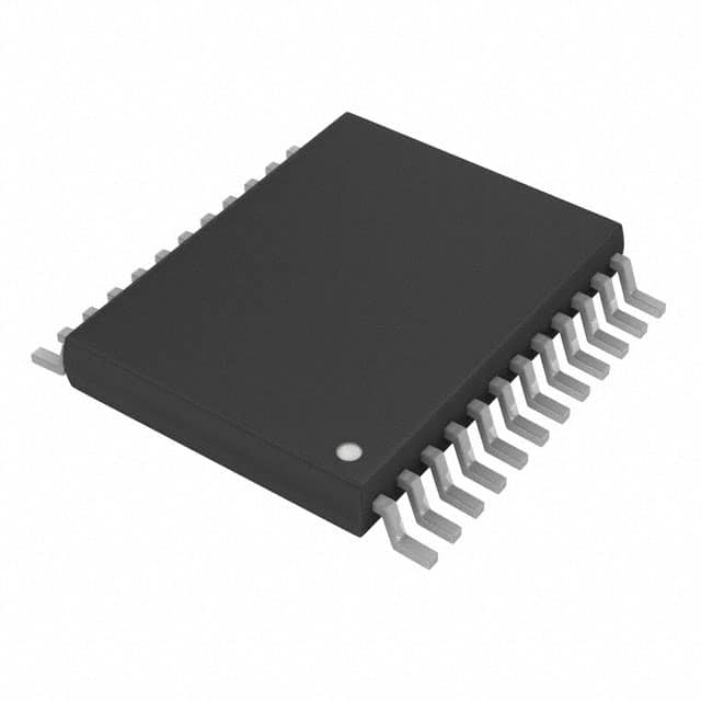
- Package: VSSOP-20
- Essence: A versatile IC used for signal routing and control in digital systems
- Packaging/Quantity: Tape and Reel, 2500 units per reel
Specifications
- Supply Voltage Range: 1.65V to 3.6V
- On-State Resistance: 4Ω (typical)
- Bandwidth: 400MHz (typical)
- Number of Channels: 16
- Input/Output Capacitance: 2pF (typical)
- Operating Temperature Range: -40°C to +85°C
Detailed Pin Configuration
The SN74CBTLV3861DGVR has a VSSOP-20 package with the following pin configuration:
- Channel 0 Control (C0)
- Channel 1 Control (C1)
- Channel 2 Control (C2)
- Channel 3 Control (C3)
- Channel 4 Control (C4)
- Channel 5 Control (C5)
- Channel 6 Control (C6)
- Channel 7 Control (C7)
- Channel 8 Control (C8)
- Channel 9 Control (C9)
- Channel 10 Control (C10)
- Channel 11 Control (C11)
- Channel 12 Control (C12)
- Channel 13 Control (C13)
- Channel 14 Control (C14)
- Channel 15 Control (C15)
- Ground (GND)
- Channel Select (S)
- Output Enable (OE)
- Power Supply (VCC)
Functional Features
- Low voltage operation allows compatibility with a wide range of digital systems.
- High-speed switching enables efficient signal routing in time-critical applications.
- Low power consumption reduces energy requirements and extends battery life.
- Wide bandwidth ensures accurate transmission of high-frequency signals.
- Multiple channels provide flexibility for signal multiplexing and demultiplexing.
Advantages and Disadvantages
Advantages: - Versatile IC suitable for various digital applications. - Low voltage operation allows integration into different voltage domains. - High-speed switching enables real-time signal routing. - Low power consumption reduces energy costs and heat dissipation. - Compact package size saves board space.
Disadvantages: - Limited number of channels may not be sufficient for complex systems. - On-state resistance may introduce signal attenuation. - Sensitivity to electrostatic discharge (ESD) requires proper handling precautions.
Working Principles
The SN74CBTLV3861DGVR is a digital multiplexer/demultiplexer IC that operates by selectively connecting input signals to output channels based on control inputs. The channel select (S) pin determines the active channel, while the channel control pins (C0-C15) enable or disable individual channels. The output enable (OE) pin controls the output state.
When a specific channel is selected, the corresponding control pin activates the internal switch, connecting the input signal to the output pin. The low on-state resistance ensures minimal signal distortion during transmission. The IC operates within a specified supply voltage range and can handle high-frequency signals due to its wide bandwidth.
Detailed Application Field Plans
The SN74CBTLV3861DGVR finds applications in various digital systems, including:
- Communication Systems: Used for signal routing in telecommunication networks, such as multiplexing/demultiplexing data streams in optical communication systems.
- Data Acquisition Systems: Enables selection and routing of analog and digital signals in data acquisition systems, ensuring accurate measurement and control.
- Test and Measurement Equipment: Provides signal routing capabilities in test and measurement equipment, allowing efficient testing and analysis of electronic devices.
- Consumer Electronics: Used in audio/video systems, gaming consoles, and other consumer electronics for signal switching and control.
- Industrial Automation: Enables signal routing and control in industrial automation systems, facilitating efficient process control and monitoring.
Detailed and Complete Alternative Models
- SN74CBTLV3257: 4-Bit FET Multiplexer/Demultiplexer with 5V Tolerant Inputs/Outputs
- SN74CBT16212: 24-Bit FET Bus Switch
- SN74CBT3244: 8-Bit FET Bus Switch
- SN74CBT3384: 10-Bit FET Bus Switch
- SN74CBT3257: 4-Bit FET Multiplexer/Demultiplexer
These alternative models offer similar functionality and can be considered based on specific application requirements.
Word count: 530 words
Liệt kê 10 câu hỏi và câu trả lời thường gặp liên quan đến ứng dụng SN74CBTLV3861DGVR trong giải pháp kỹ thuật
Sure! Here are 10 common questions and answers related to the application of SN74CBTLV3861DGVR:
Q1: What is SN74CBTLV3861DGVR? A1: SN74CBTLV3861DGVR is a specific integrated circuit (IC) that functions as a high-bandwidth switch for digital signals.
Q2: What is the purpose of SN74CBTLV3861DGVR? A2: The purpose of SN74CBTLV3861DGVR is to enable the routing of digital signals between different components or subsystems in a technical solution.
Q3: What voltage levels does SN74CBTLV3861DGVR support? A3: SN74CBTLV3861DGVR supports voltage levels ranging from 1.65V to 3.6V.
Q4: How many channels does SN74CBTLV3861DGVR have? A4: SN74CBTLV3861DGVR has a total of 10 channels, allowing it to switch multiple digital signals simultaneously.
Q5: What is the maximum data rate supported by SN74CBTLV3861DGVR? A5: SN74CBTLV3861DGVR can handle data rates up to 400 Mbps.
Q6: Can SN74CBTLV3861DGVR be used for bidirectional signal routing? A6: Yes, SN74CBTLV3861DGVR supports bidirectional signal routing, making it suitable for applications where signals need to be transmitted in both directions.
Q7: Is SN74CBTLV3861DGVR compatible with different logic families? A7: Yes, SN74CBTLV3861DGVR is compatible with various logic families, including TTL, CMOS, and LVCMOS.
Q8: What is the power supply voltage range for SN74CBTLV3861DGVR? A8: SN74CBTLV3861DGVR operates with a power supply voltage range of 1.65V to 3.6V.
Q9: Can SN74CBTLV3861DGVR be used in battery-powered applications? A9: Yes, SN74CBTLV3861DGVR's low power consumption makes it suitable for battery-powered applications.
Q10: Are there any specific application notes or reference designs available for SN74CBTLV3861DGVR? A10: Yes, Texas Instruments provides application notes and reference designs that can help users implement SN74CBTLV3861DGVR effectively in their technical solutions.
Please note that these questions and answers are general and may vary depending on specific use cases and requirements.