

Xem thông số kỹ thuật để biết chi tiết sản phẩm.
SN74LV244ATDGVRE4
Product Overview
- Category: Integrated Circuit (IC)
- Use: Buffer/Line Driver
- Characteristics: Low-voltage, Octal Bus Buffer with 3-State Outputs
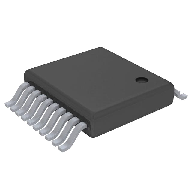
- Package: TSSOP-20
- Essence: This IC is designed to provide buffering and line driving capabilities for digital signals in low-voltage applications.
- Packaging/Quantity: Tape and Reel, 2500 units per reel
Specifications
- Supply Voltage Range: 1.65V to 5.5V
- Input Voltage Range: 0V to VCC
- Output Voltage Range: 0V to VCC
- High-Level Input Voltage: 0.7 x VCC to VCC
- Low-Level Input Voltage: 0V to 0.3 x VCC
- High-Level Output Voltage: 0.9 x VCC to VCC
- Low-Level Output Voltage: 0V to 0.1 x VCC
- Maximum Operating Frequency: 100MHz
- Number of Channels: 8
- Output Type: 3-State
Detailed Pin Configuration
The SN74LV244ATDGVRE4 has a TSSOP-20 package with the following pin configuration:
__    __
   A1 | 1    20 | VCC
   B1 | 2    19 | OE#
   A2 | 3    18 | B2
   B2 | 4    17 | A3
   A3 | 5    16 | B3
   B3 | 6    15 | A4
   GND| 7    14 | B4
   Y1 | 8    13 | A5
   Y2 | 9    12 | B5
   A5 |10    11 | Y3
       ‾‾    ‾‾
Functional Features
- Octal buffer with 3-state outputs
- Provides non-inverting level shifting and line driving capabilities
- Enables bidirectional communication between different voltage domains
- Supports low-voltage applications with a wide supply voltage range
- Offers high-speed operation with a maximum frequency of 100MHz
- Allows for easy interfacing with microcontrollers, FPGAs, and other digital devices
Advantages and Disadvantages
Advantages: - Wide supply voltage range allows for compatibility with various systems - High-speed operation enables efficient data transfer - 3-state outputs provide flexibility in controlling bus lines - Small package size saves board space
Disadvantages: - Limited number of channels (8) - Not suitable for high-power applications
Working Principles
The SN74LV244ATDGVRE4 operates by receiving digital input signals on its A1-A5 and B1-B5 pins. These inputs are then buffered and amplified to drive the corresponding Y1-Y3 outputs. The OE# pin is used to enable or disable the outputs. When OE# is low, the outputs are active and reflect the input signals. When OE# is high, the outputs are in a high-impedance state, allowing other devices to control the bus lines.
Detailed Application Field Plans
The SN74LV244ATDGVRE4 is commonly used in various applications, including:
- Microcontroller interfacing: It facilitates communication between microcontrollers operating at different voltage levels.
- FPGA I/O expansion: It provides additional I/O lines for field-programmable gate arrays (FPGAs) to interface with external devices.
- Level shifting: It converts logic levels between different voltage domains, enabling compatibility between incompatible systems.
- Bus driving: It drives bus lines in digital systems, ensuring reliable signal transmission.
Detailed and Complete Alternative Models
- SN74LV244A: Similar to SN74LV244ATDGVRE4 but with a different package (SOIC-20).
- SN74LVC244A: Low-voltage octal buffer with 3-state outputs, compatible with 3.3V systems.
- SN74HCT244: Octal buffer with 3-state outputs, suitable for high-speed applications.
These alternative models offer similar functionality and can be used as replacements depending on specific requirements.
Word count: 446 words
Liệt kê 10 câu hỏi và câu trả lời thường gặp liên quan đến ứng dụng SN74LV244ATDGVRE4 trong giải pháp kỹ thuật
What is the operating voltage range of SN74LV244ATDGVRE4?
- The operating voltage range of SN74LV244ATDGVRE4 is 1.65V to 5.5V.What is the maximum output current of SN74LV244ATDGVRE4?
- The maximum output current per channel of SN74LV244ATDGVRE4 is ±12mA.Can SN74LV244ATDGVRE4 be used in automotive applications?
- Yes, SN74LV244ATDGVRE4 is qualified for automotive applications.What is the typical propagation delay of SN74LV244ATDGVRE4?
- The typical propagation delay of SN74LV244ATDGVRE4 is 6ns at 3.3V.Is SN74LV244ATDGVRE4 compatible with 5V TTL input levels?
- Yes, SN74LV244ATDGVRE4 is compatible with 5V TTL input levels.Does SN74LV244ATDGVRE4 have overvoltage-tolerant inputs?
- Yes, SN74LV244ATDGVRE4 has overvoltage-tolerant inputs.What is the package type of SN74LV244ATDGVRE4?
- SN74LV244ATDGVRE4 is available in a 20-pin TSSOP package.Can SN74LV244ATDGVRE4 be used in bidirectional level-shifting applications?
- Yes, SN74LV244ATDGVRE4 can be used in bidirectional level-shifting applications.What is the maximum operating frequency of SN74LV244ATDGVRE4?
- The maximum operating frequency of SN74LV244ATDGVRE4 is 80MHz.Is SN74LV244ATDGVRE4 RoHS compliant?
- Yes, SN74LV244ATDGVRE4 is RoHS compliant.