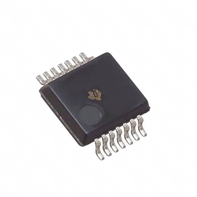
Xem thông số kỹ thuật để biết chi tiết sản phẩm.

SN74LVC06ADBR
Product Overview
- Category: Integrated Circuit (IC)
- Use: Logic Gate Inverter
- Characteristics: Low-Voltage CMOS, Hex Inverter
- Package: SSOP-14
- Essence: The SN74LVC06ADBR is a hex inverter IC that operates at low voltage levels and is designed using complementary metal-oxide-semiconductor (CMOS) technology.
- Packaging/Quantity: Each package contains 200 units.
Specifications
- Supply Voltage: 1.65V to 5.5V
- Input Voltage: 0V to VCC
- Output Voltage: 0V to VCC
- Operating Temperature Range: -40°C to +85°C
- Propagation Delay: 3.8ns (typical)
- Output Drive Capability: ±24mA
Pin Configuration
The SN74LVC06ADBR has a total of 14 pins arranged as follows:
__    __
   Y1 |1  \__/ 14| VCC
   A1 |2        13| A6
   B1 |3        12| B6
   A2 |4   SN   11| A5
   B2 |5   74   10| B5
   Y2 |6   LVC   9| Y5
  GND |7        8| GND
       ----------
Functional Features
- Hex Inverter: The SN74LVC06ADBR consists of six independent inverters, each capable of converting a logic high input to a logic low output and vice versa.
- Low-Voltage Operation: It can operate at low supply voltages ranging from 1.65V to 5.5V, making it suitable for low-power applications.
- CMOS Technology: The IC is designed using CMOS technology, which provides high noise immunity and low power consumption.
- High-Speed Operation: With a propagation delay of only 3.8ns (typical), the SN74LVC06ADBR ensures fast signal processing.
Advantages and Disadvantages
Advantages
- Low-voltage operation allows for compatibility with various systems.
- High-speed operation enables quick signal processing.
- CMOS technology provides high noise immunity and low power consumption.
Disadvantages
- Limited output drive capability may restrict its use in applications requiring higher current levels.
- The SSOP-14 package may not be suitable for all PCB designs.
Working Principles
The SN74LVC06ADBR operates as a hex inverter by utilizing complementary MOS transistors. When an input signal is applied to one of the inverters, the internal circuitry switches the output to the opposite logic level. This inversion process occurs due to the characteristics of the MOS transistors used in the design.
Detailed Application Field Plans
The SN74LVC06ADBR can be used in various applications, including:
- Digital Logic Circuits: It can be employed as a basic building block for constructing complex digital logic circuits.
- Signal Level Shifting: The hex inverter can be utilized to shift signal levels between different voltage domains.
- Oscillator Circuits: By combining multiple inverters, the IC can be used to generate clock signals in oscillator circuits.
- Voltage Level Conversion: It can convert logic levels between different voltage standards, facilitating compatibility between different systems.
Detailed and Complete Alternative Models
- SN74LVC04A: Hex Inverter IC with similar characteristics but in a different package (SOIC-14).
- CD4069UB: Hex Inverter IC with comparable specifications and functionality, but from a different manufacturer (Texas Instruments).
These alternative models can be considered based on specific requirements, availability, and compatibility with the target application.
Word count: 436 words
Liệt kê 10 câu hỏi và câu trả lời thường gặp liên quan đến ứng dụng SN74LVC06ADBR trong giải pháp kỹ thuật
Sure! Here are 10 common questions and answers related to the application of SN74LVC06ADBR:
Q: What is SN74LVC06ADBR? A: SN74LVC06ADBR is a hex inverter with open-drain outputs, which means it can invert input signals and drive them as open-drain outputs.
Q: What is the voltage range supported by SN74LVC06ADBR? A: SN74LVC06ADBR supports a voltage range from 1.65V to 5.5V.
Q: What is the maximum output current of SN74LVC06ADBR? A: The maximum output current of SN74LVC06ADBR is typically 32mA.
Q: Can SN74LVC06ADBR be used for level shifting between different voltage domains? A: Yes, SN74LVC06ADBR can be used for level shifting between different voltage domains due to its wide voltage range support.
Q: How many inverters are there in SN74LVC06ADBR? A: SN74LVC06ADBR consists of six independent inverters.
Q: What is the propagation delay of SN74LVC06ADBR? A: The propagation delay of SN74LVC06ADBR is typically around 4.3ns.
Q: Can SN74LVC06ADBR tolerate overvoltage conditions? A: No, SN74LVC06ADBR is not designed to tolerate overvoltage conditions. It is recommended to stay within the specified voltage range.
Q: Is SN74LVC06ADBR suitable for high-speed applications? A: Yes, SN74LVC06ADBR is suitable for high-speed applications as it has a fast propagation delay and supports a wide voltage range.
Q: Can SN74LVC06ADBR be used in both digital and analog circuits? A: SN74LVC06ADBR is primarily designed for digital circuits, but it can also be used in certain analog applications.
Q: What is the package type of SN74LVC06ADBR? A: SN74LVC06ADBR is available in a small-outline integrated circuit (SOIC) package with 14 pins.
Please note that these answers are general and may vary depending on specific application requirements.

