Xem thông số kỹ thuật để biết chi tiết sản phẩm.

SN74LVC1G08DCKT
Product Overview
Category
SN74LVC1G08DCKT belongs to the category of integrated circuits (ICs).
Use
It is commonly used as a logic gate in digital electronic circuits.
Characteristics
- Low-voltage CMOS technology
- High-speed operation
- Low power consumption
- Wide operating voltage range
- Small package size
Package
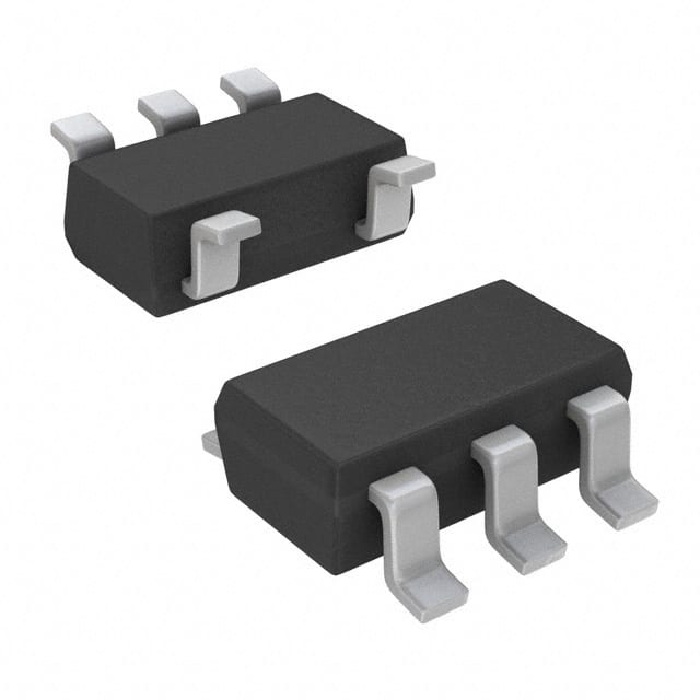
SN74LVC1G08DCKT is available in a small SOT-23-5 package.
Essence
The essence of SN74LVC1G08DCKT lies in its ability to perform logical AND operations on two input signals.
Packaging/Quantity
SN74LVC1G08DCKT is typically sold in reels, with each reel containing 3000 units.
Specifications
- Supply Voltage: 1.65V to 5.5V
- Input Voltage Range: 0V to VCC
- Output Voltage Range: 0V to VCC
- Operating Temperature Range: -40°C to +85°C
- Propagation Delay: 3.8ns (typical)
- Maximum Quiescent Current: 10µA
Detailed Pin Configuration
SN74LVC1G08DCKT has a total of five pins:
- GND (Ground): Connected to the ground reference potential.
- A (Input A): First input signal for the logical AND operation.
- B (Input B): Second input signal for the logical AND operation.
- Y (Output): Output signal representing the result of the logical AND operation.
- VCC (Supply Voltage): Connected to the positive supply voltage.
Functional Features
SN74LVC1G08DCKT offers the following functional features:
- Performs logical AND operation on two input signals (A and B).
- Provides a single output signal (Y) based on the logical AND operation result.
- High-speed operation allows for efficient processing of input signals.
- Low power consumption makes it suitable for battery-powered devices.
- Wide operating voltage range enables compatibility with various systems.
Advantages and Disadvantages
Advantages
- Small package size saves board space in compact designs.
- Low power consumption extends battery life in portable devices.
- Wide operating voltage range provides flexibility in different applications.
- High-speed operation ensures efficient signal processing.
Disadvantages
- Limited number of inputs (only two) restricts complex logic operations.
- Sensitive to electrostatic discharge (ESD), requiring proper handling precautions.
Working Principles
SN74LVC1G08DCKT operates based on the principles of CMOS technology. It utilizes MOSFET transistors to perform logical AND operations on the input signals. The internal circuitry consists of multiple stages, including inverters and pass gates, which enable the desired logic functionality.
Detailed Application Field Plans
SN74LVC1G08DCKT finds applications in various fields, including:
- Consumer Electronics: Used in smartphones, tablets, and wearable devices for logic operations.
- Automotive: Employed in automotive electronics for signal processing and control functions.
- Industrial Automation: Integrated into control systems and PLCs for logical operations.
- Communication Systems: Utilized in networking equipment and data transmission devices.
- Medical Devices: Incorporated into medical instruments for logic-based decision-making.
Detailed and Complete Alternative Models
Some alternative models that offer similar functionality to SN74LVC1G08DCKT are:
- 74HC08: A popular alternative from the HC family of logic gates.
- CD4081: A CMOS-based quad 2-input AND gate.
- SN74LS08: A TTL-based quad 2-input AND gate.
These alternatives can be considered based on specific requirements and compatibility with existing designs.
Word count: 497 words
Liệt kê 10 câu hỏi và câu trả lời thường gặp liên quan đến ứng dụng SN74LVC1G08DCKT trong giải pháp kỹ thuật
Sure! Here are 10 common questions and answers related to the application of SN74LVC1G08DCKT:
Q1: What is SN74LVC1G08DCKT? A1: SN74LVC1G08DCKT is a single 2-input AND gate IC (integrated circuit) from Texas Instruments.
Q2: What is the voltage supply range for SN74LVC1G08DCKT? A2: The voltage supply range for SN74LVC1G08DCKT is typically between 1.65V and 5.5V.
Q3: What is the maximum output current of SN74LVC1G08DCKT? A3: The maximum output current of SN74LVC1G08DCKT is 32mA.
Q4: Can SN74LVC1G08DCKT be used in battery-powered applications? A4: Yes, SN74LVC1G08DCKT can be used in battery-powered applications due to its low power consumption.
Q5: What is the operating temperature range for SN74LVC1G08DCKT? A5: The operating temperature range for SN74LVC1G08DCKT is typically between -40°C and 125°C.
Q6: How many inputs does SN74LVC1G08DCKT have? A6: SN74LVC1G08DCKT has two inputs.
Q7: Can SN74LVC1G08DCKT be used as a level shifter? A7: Yes, SN74LVC1G08DCKT can be used as a level shifter to convert signals between different voltage levels.
Q8: What is the propagation delay of SN74LVC1G08DCKT? A8: The propagation delay of SN74LVC1G08DCKT is typically around 3.5ns.
Q9: Can SN74LVC1G08DCKT be used in high-speed applications? A9: Yes, SN74LVC1G08DCKT can be used in high-speed applications due to its fast switching speed.
Q10: Is SN74LVC1G08DCKT available in a surface-mount package? A10: Yes, SN74LVC1G08DCKT is available in a surface-mount package (SC-70).

