

Xem thông số kỹ thuật để biết chi tiết sản phẩm.
SN74LVC1G34YZVR
Product Overview
- Category: Integrated Circuit (IC)
- Use: Logic Gate
- Characteristics:
- Low-voltage CMOS technology
- Single gate buffer
- High-speed operation
- Wide operating voltage range
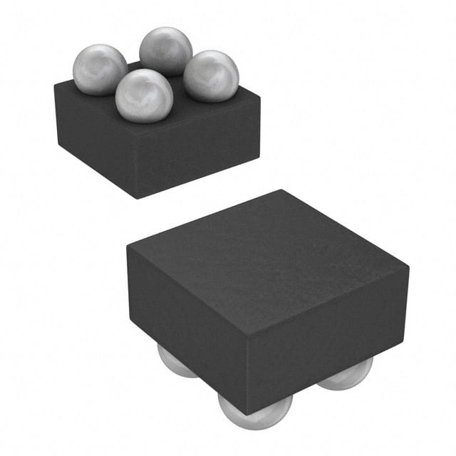
- Package: SOT-553
- Essence: Buffer gate
- Packaging/Quantity: Tape and Reel, 3000 pieces per reel
Specifications
- Supply Voltage Range: 1.65V to 5.5V
- Input Voltage Range: 0V to VCC
- Output Voltage Range: 0V to VCC
- Operating Temperature Range: -40°C to +125°C
- Propagation Delay: 3.8ns (typical) at 3.3V
- Maximum Quiescent Current: 10μA at 5.5V
- Maximum Output Current: ±32mA
Detailed Pin Configuration
The SN74LVC1G34YZVR has the following pin configuration:
____
   A -|    |- VCC
   Y -|    |- GND
   B -|____|
Functional Features
- Single gate buffer with Schmitt-trigger inputs
- Converts slow input signals into fast output signals
- Provides signal buffering and level shifting capabilities
- Suitable for voltage level translation applications
- High noise immunity due to Schmitt-trigger inputs
Advantages and Disadvantages
Advantages: - Low-voltage operation allows compatibility with a wide range of systems - High-speed operation enables efficient signal processing - Small package size saves board space - Schmitt-trigger inputs provide noise immunity
Disadvantages: - Limited number of gates in a single package - Not suitable for high-current applications
Working Principles
The SN74LVC1G34YZVR is a single gate buffer that operates using low-voltage CMOS technology. It takes an input signal and converts it into a fast output signal. The Schmitt-trigger inputs ensure high noise immunity by providing hysteresis, making the device less susceptible to voltage fluctuations and noise.
Detailed Application Field Plans
The SN74LVC1G34YZVR can be used in various applications, including but not limited to: - Signal level shifting in mixed voltage systems - Buffering weak signals from sensors or switches - Voltage level translation between different logic families - Clock signal buffering in digital circuits - Input signal conditioning in communication systems
Detailed and Complete Alternative Models
Some alternative models that offer similar functionality to the SN74LVC1G34YZVR are: - 74LVC1G34GW,125 - NC7SZ34P5X - TC7SZ34FU
These alternatives provide comparable features and can be used as replacements depending on specific requirements.
Word count: 274
Liệt kê 10 câu hỏi và câu trả lời thường gặp liên quan đến ứng dụng SN74LVC1G34YZVR trong giải pháp kỹ thuật
Sure! Here are 10 common questions and answers related to the application of SN74LVC1G34YZVR in technical solutions:
Q1: What is SN74LVC1G34YZVR? A1: SN74LVC1G34YZVR is a single buffer gate IC (integrated circuit) that can be used for level shifting, signal buffering, and voltage translation applications.
Q2: What is the operating voltage range of SN74LVC1G34YZVR? A2: SN74LVC1G34YZVR operates within a voltage range of 1.65V to 5.5V.
Q3: What is the maximum output current of SN74LVC1G34YZVR? A3: The maximum output current of SN74LVC1G34YZVR is typically around 32mA.
Q4: Can SN74LVC1G34YZVR be used for bidirectional level shifting? A4: No, SN74LVC1G34YZVR is a unidirectional buffer gate and cannot be used for bidirectional level shifting.
Q5: What is the propagation delay of SN74LVC1G34YZVR? A5: The propagation delay of SN74LVC1G34YZVR is typically around 3.8ns.
Q6: Can SN74LVC1G34YZVR handle high-speed signals? A6: Yes, SN74LVC1G34YZVR is designed to handle high-speed signals and can operate at frequencies up to several hundred megahertz.
Q7: Is SN74LVC1G34YZVR compatible with both CMOS and TTL logic levels? A7: Yes, SN74LVC1G34YZVR is compatible with both CMOS (Complementary Metal-Oxide-Semiconductor) and TTL (Transistor-Transistor Logic) logic levels.
Q8: Can SN74LVC1G34YZVR be used for voltage level translation between different supply voltages? A8: Yes, SN74LVC1G34YZVR can be used for voltage level translation between different supply voltages, as long as the voltage levels are within its operating range.
Q9: What is the package type of SN74LVC1G34YZVR? A9: SN74LVC1G34YZVR is available in a small SOT-23-5 package.
Q10: Are there any recommended applications for SN74LVC1G34YZVR? A10: SN74LVC1G34YZVR is commonly used in applications such as signal buffering, level shifting, clock distribution, and general-purpose logic gate functions.
Please note that these answers are general and may vary depending on specific datasheet specifications and application requirements.