

Xem thông số kỹ thuật để biết chi tiết sản phẩm.
SN74LVC2G17YZPR
Basic Information Overview
- Category: Integrated Circuit (IC)
- Use: Logic Gate
- Characteristics: Dual Schmitt-Trigger Buffer/Driver
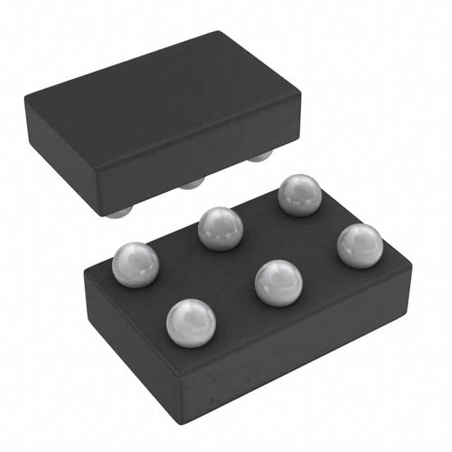
- Package: 8-pin DSBGA (MicroStar Junior™) package
- Essence: High-speed, low-power consumption buffer/driver
- Packaging/Quantity: Tape and Reel, 3000 units per reel
Specifications
- Supply Voltage Range: 1.65V to 5.5V
- Input Voltage Range: 0V to VCC
- Output Voltage Range: 0V to VCC
- High-Level Input Voltage: 0.7 x VCC to VCC
- Low-Level Input Voltage: 0V to 0.3 x VCC
- High-Level Output Voltage: 0.9 x VCC to VCC
- Low-Level Output Voltage: 0V to 0.1 x VCC
- Maximum Operating Frequency: 100 MHz
- Propagation Delay: 4.6 ns (typical)
Detailed Pin Configuration
The SN74LVC2G17YZPR has the following pin configuration:
___________
   1 -| A         |-
   2 -| Y         |-
   3 -| GND       |-
   4 -| B         |-
   5 -| Y         |-
   6 -| VCC       |-
   7 -| NC        |-
   8 -| Y         |-
       -----------
Functional Features
- Dual Schmitt-trigger buffer/driver with open-drain outputs
- Wide supply voltage range allows compatibility with various systems
- High-speed operation suitable for applications requiring fast signal propagation
- Low power consumption for energy-efficient designs
- Schmitt-trigger inputs provide hysteresis, ensuring noise immunity and signal integrity
Advantages
- Compact 8-pin package saves board space
- High-speed operation enables efficient data transmission
- Low power consumption extends battery life in portable devices
- Schmitt-trigger inputs enhance noise immunity, reducing errors in noisy environments
Disadvantages
- Limited number of input/output pins may restrict complex circuit designs
- Open-drain outputs require external pull-up resistors for proper signal levels
Working Principles
The SN74LVC2G17YZPR is a dual Schmitt-trigger buffer/driver. It accepts two input signals (A and B) and provides three output signals (Y). The Schmitt-trigger inputs ensure that the output transitions occur at different voltage levels for rising and falling input signals, providing noise immunity and preventing false triggering. The open-drain outputs require external pull-up resistors to establish the desired logic levels.
Detailed Application Field Plans
The SN74LVC2G17YZPR is commonly used in various applications, including: 1. Communication systems: Signal buffering and level shifting in UART, SPI, and I2C interfaces. 2. Industrial automation: Driving sensors, actuators, and relays in control systems. 3. Automotive electronics: Signal conditioning and interfacing in automotive modules. 4. Consumer electronics: Logic-level translation and buffering in smartphones, tablets, and gaming consoles. 5. Medical devices: Signal amplification and isolation in medical monitoring equipment.
Detailed and Complete Alternative Models
- SN74LVC2G07DCTR: Dual Buffer/Driver with Open-Drain Outputs, SOT-23 package.
- SN74LVC2G34DCUR: Dual Buffer/Driver with Schmitt-Trigger Inputs, USON-6 package.
- SN74LVC2G14DCKR: Dual Inverter with Schmitt-Trigger Inputs, SC-70 package.
- SN74LVC2G125DCUR: Dual Bus Buffer/Driver with 3-State Outputs, USON-6 package.
These alternative models offer similar functionality and can be used as substitutes for the SN74LVC2G17YZPR in various applications.
Word count: 446 words
Liệt kê 10 câu hỏi và câu trả lời thường gặp liên quan đến ứng dụng SN74LVC2G17YZPR trong giải pháp kỹ thuật
Sure! Here are 10 common questions and answers related to the application of SN74LVC2G17YZPR:
Q: What is the SN74LVC2G17YZPR? A: The SN74LVC2G17YZPR is a dual Schmitt-trigger buffer/driver integrated circuit (IC) that can be used in various technical solutions.
Q: What is the purpose of the SN74LVC2G17YZPR? A: The SN74LVC2G17YZPR is designed to provide signal buffering and driving capabilities, particularly useful for applications involving voltage level shifting or noise immunity enhancement.
Q: What is a Schmitt-trigger? A: A Schmitt-trigger is a circuit that converts an input signal into a digital output signal with hysteresis, which helps improve noise immunity and signal integrity.
Q: What are the voltage levels supported by the SN74LVC2G17YZPR? A: The SN74LVC2G17YZPR supports voltage levels from 1.65V to 5.5V, making it compatible with a wide range of digital systems.
Q: How many channels does the SN74LVC2G17YZPR have? A: The SN74LVC2G17YZPR has two independent channels, allowing it to buffer or drive two separate signals simultaneously.
Q: Can the SN74LVC2G17YZPR be used for bidirectional communication? A: No, the SN74LVC2G17YZPR is a unidirectional buffer/driver and does not support bidirectional communication.
Q: What is the maximum output current of the SN74LVC2G17YZPR? A: The SN74LVC2G17YZPR can provide a maximum output current of 32mA, which is suitable for driving standard logic levels.
Q: Is the SN74LVC2G17YZPR capable of handling high-speed signals? A: Yes, the SN74LVC2G17YZPR has a propagation delay of only a few nanoseconds, making it suitable for high-speed applications.
Q: Can the SN74LVC2G17YZPR tolerate overvoltage or undervoltage conditions? A: The SN74LVC2G17YZPR has built-in protection features that help it tolerate overvoltage and undervoltage conditions, enhancing its robustness.
Q: What package does the SN74LVC2G17YZPR come in? A: The SN74LVC2G17YZPR is available in a small footprint, industry-standard package known as DSBGA (MicroStar Junior™), which facilitates easy integration into various designs.
Please note that these answers are general and may vary depending on specific application requirements.