

Xem thông số kỹ thuật để biết chi tiết sản phẩm.
SN74LVC2G53YEPR
Product Overview
- Category: Integrated Circuit (IC)
- Use: Logic Gate
- Characteristics: Dual 2-Input Multiplexer
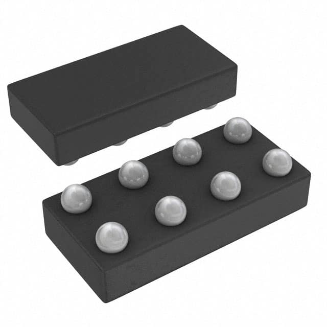
- Package: 8-pin VSSOP
- Essence: High-speed CMOS technology
- Packaging/Quantity: Tape and Reel, 2500 units per reel
Specifications
- Supply Voltage Range: 1.65V to 5.5V
- Input Voltage Range: 0V to VCC
- Output Voltage Range: 0V to VCC
- High-Speed Operation: tPD = 3.8ns (typ) at 3.3V
- Low Power Consumption: ICC = 1µA (max) at TA = 25°C
- Operating Temperature Range: -40°C to +85°C
Detailed Pin Configuration
The SN74LVC2G53YEPR has the following pin configuration:
___________
      |           |
   A1 |1        8| VCC
   B1 |2        7| Y
   S1 |3        6| B2
  GND |4        5| A2
      |___________|
Functional Features
- Dual 2-input multiplexer with common select input (S1)
- Selects one of two data inputs (A1 or B1) based on the value of S1
- Outputs the selected data on the Y output pin
- High-speed operation allows for efficient data switching
- Low power consumption ensures energy efficiency
Advantages and Disadvantages
Advantages: - High-speed operation enables quick data processing - Low power consumption reduces energy usage - Compact package size saves board space - Wide supply voltage range allows for versatile applications
Disadvantages: - Limited number of inputs and outputs - Not suitable for applications requiring more complex logic functions
Working Principles
The SN74LVC2G53YEPR is a dual 2-input multiplexer that operates based on the value of the select input (S1). When S1 is low, data input A1 is selected and outputted on pin Y. Conversely, when S1 is high, data input B1 is selected and outputted on pin Y. The high-speed CMOS technology used in this IC ensures efficient data switching, while the low power consumption enhances energy efficiency.
Detailed Application Field Plans
The SN74LVC2G53YEPR can be used in various applications, including but not limited to: - Data routing and selection in digital systems - Signal conditioning and multiplexing in communication systems - Address decoding in memory systems - Logic level conversion in mixed voltage systems
Detailed and Complete Alternative Models
Some alternative models that offer similar functionality to the SN74LVC2G53YEPR include: - CD4053B: Triple 2-channel analog multiplexer/demultiplexer - MC14051B: 8-channel analog multiplexer/demultiplexer - 74HC157: Quad 2-input multiplexer
These alternative models provide different options in terms of channel count and additional features, allowing users to choose the most suitable option for their specific application requirements.
Word count: 346 words
Liệt kê 10 câu hỏi và câu trả lời thường gặp liên quan đến ứng dụng SN74LVC2G53YEPR trong giải pháp kỹ thuật
Sure! Here are 10 common questions and answers related to the application of SN74LVC2G53YEPR in technical solutions:
Q: What is the SN74LVC2G53YEPR? A: The SN74LVC2G53YEPR is a dual 2-input multiplexer IC (Integrated Circuit) that can be used for signal routing and selection in various electronic applications.
Q: What is the operating voltage range of SN74LVC2G53YEPR? A: The operating voltage range of SN74LVC2G53YEPR is typically between 1.65V and 5.5V, making it compatible with a wide range of digital systems.
Q: How many inputs does SN74LVC2G53YEPR have? A: SN74LVC2G53YEPR has two independent input channels, each with two input pins.
Q: What is the output configuration of SN74LVC2G53YEPR? A: SN74LVC2G53YEPR has one output pin per channel, providing a single output for each input channel.
Q: Can SN74LVC2G53YEPR handle analog signals? A: No, SN74LVC2G53YEPR is designed specifically for digital signals and is not suitable for handling analog signals.
Q: What is the maximum data rate supported by SN74LVC2G53YEPR? A: SN74LVC2G53YEPR can support data rates up to 400 Mbps, making it suitable for high-speed digital applications.
Q: Does SN74LVC2G53YEPR have any built-in protection features? A: Yes, SN74LVC2G53YEPR has built-in ESD (Electrostatic Discharge) protection, which helps safeguard the IC against electrostatic damage during handling and operation.
Q: Can SN74LVC2G53YEPR be used in battery-powered applications? A: Yes, SN74LVC2G53YEPR's low power consumption and wide operating voltage range make it suitable for battery-powered applications.
Q: What is the package type of SN74LVC2G53YEPR? A: SN74LVC2G53YEPR is available in a small SOT-23 package, which is compact and suitable for space-constrained designs.
Q: Are there any application notes or reference designs available for SN74LVC2G53YEPR? A: Yes, Texas Instruments provides application notes and reference designs that can help users understand and implement SN74LVC2G53YEPR in their technical solutions.
Please note that the answers provided here are general and may vary depending on specific datasheet specifications and application requirements.