

Xem thông số kỹ thuật để biết chi tiết sản phẩm.
SN74LVC823ANSRG4
Product Overview
Category
SN74LVC823ANSRG4 belongs to the category of integrated circuits (ICs).
Use
This IC is commonly used in digital logic applications.
Characteristics
- Low voltage CMOS technology
- High-speed operation
- Wide operating voltage range
- Low power consumption
- Schmitt-trigger inputs for noise immunity
- 8-bit transparent latch with 3-state outputs
Package
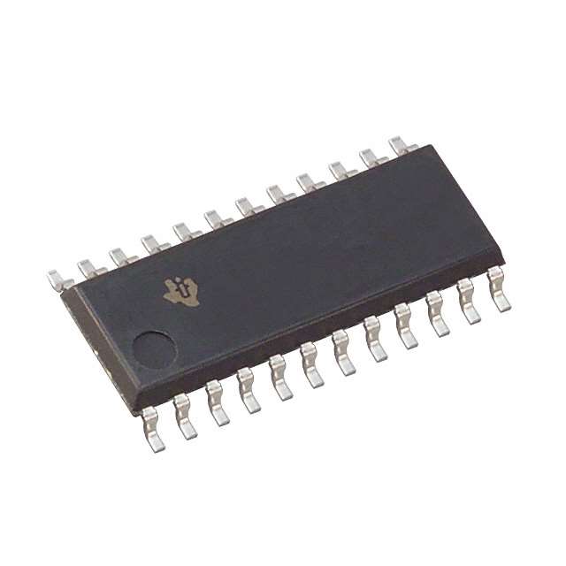
SN74LVC823ANSRG4 is available in a small-outline package (SOIC) with a nominal dimension of 5.3mm x 6.2mm.
Essence
The essence of SN74LVC823ANSRG4 lies in its ability to provide reliable and efficient digital logic functionality in various electronic systems.
Packaging/Quantity
This IC is typically packaged in reels, with each reel containing a specific quantity of units. The exact packaging and quantity can vary depending on the supplier.
Specifications
- Supply Voltage Range: 1.65V to 3.6V
- Input Voltage Range: 0V to VCC
- Output Voltage Range: 0V to VCC
- Operating Temperature Range: -40°C to +85°C
- Maximum Propagation Delay Time: 4.3ns
- Maximum Quiescent Current: 10μA
Detailed Pin Configuration
The SN74LVC823ANSRG4 IC has a total of 20 pins. The pin configuration is as follows:
- GND (Ground)
- D0 (Data Input 0)
- D1 (Data Input 1)
- D2 (Data Input 2)
- D3 (Data Input 3)
- D4 (Data Input 4)
- D5 (Data Input 5)
- D6 (Data Input 6)
- D7 (Data Input 7)
- OE (Output Enable)
- LE (Latch Enable)
- Q0 (Output 0)
- Q1 (Output 1)
- Q2 (Output 2)
- Q3 (Output 3)
- Q4 (Output 4)
- Q5 (Output 5)
- Q6 (Output 6)
- Q7 (Output 7)
- VCC (Supply Voltage)
Functional Features
- 8-bit transparent latch with 3-state outputs
- Latch enable and output enable control signals for flexible operation
- Schmitt-trigger inputs for improved noise immunity
- High-speed operation for efficient data processing
- Wide operating voltage range allows compatibility with various systems
- Low power consumption for energy-efficient designs
Advantages and Disadvantages
Advantages
- Reliable and efficient digital logic functionality
- Wide operating voltage range
- Low power consumption
- Schmitt-trigger inputs for noise immunity
Disadvantages
- Limited number of outputs (8-bit)
Working Principles
SN74LVC823ANSRG4 operates based on the principles of digital logic circuits. It utilizes a latch enable signal to capture and store data from the input pins. The output enable signal controls whether the stored data is presented at the output pins or not. The Schmitt-trigger inputs ensure reliable operation by providing noise immunity.
Detailed Application Field Plans
SN74LVC823ANSRG4 finds applications in various fields, including but not limited to: - Microcontrollers - Data communication systems - Industrial automation - Consumer electronics - Automotive electronics
Detailed and Complete Alternative Models
Some alternative models that provide similar functionality to SN74LVC823ANSRG4 include: - SN74LVC4245A - SN74LVC245A - SN74LVC573A - SN74LVC541A
These alternative models offer comparable features and can be used as substitutes depending on specific requirements.
Word count: 498 words
Liệt kê 10 câu hỏi và câu trả lời thường gặp liên quan đến ứng dụng SN74LVC823ANSRG4 trong giải pháp kỹ thuật
Sure! Here are 10 common questions and answers related to the application of SN74LVC823ANSRG4:
Q: What is SN74LVC823ANSRG4? A: SN74LVC823ANSRG4 is a specific integrated circuit (IC) chip that belongs to the SN74LVC series of logic gates.
Q: What is the function of SN74LVC823ANSRG4? A: SN74LVC823ANSRG4 is an octal buffer/line driver with 3-state outputs. It can be used to amplify and drive signals in digital circuits.
Q: What voltage levels does SN74LVC823ANSRG4 support? A: SN74LVC823ANSRG4 supports voltage levels from 1.65V to 5.5V, making it compatible with a wide range of digital systems.
Q: How many inputs and outputs does SN74LVC823ANSRG4 have? A: SN74LVC823ANSRG4 has 8 inputs and 8 outputs, making it suitable for applications requiring multiple signal amplification.
Q: Can SN74LVC823ANSRG4 handle bidirectional communication? A: No, SN74LVC823ANSRG4 is a unidirectional buffer/line driver, meaning it can only amplify signals in one direction.
Q: What is the maximum output current of SN74LVC823ANSRG4? A: The maximum output current of SN74LVC823ANSRG4 is typically 24mA, allowing it to drive moderate loads.
Q: Is SN74LVC823ANSRG4 compatible with other logic families? A: Yes, SN74LVC823ANSRG4 is designed to be compatible with both TTL and CMOS logic families, making it versatile in various systems.
Q: Can SN74LVC823ANSRG4 handle high-speed signals? A: Yes, SN74LVC823ANSRG4 is capable of operating at high speeds, with a typical propagation delay of 3.5ns.
Q: Does SN74LVC823ANSRG4 have built-in protection features? A: Yes, SN74LVC823ANSRG4 has built-in ESD (electrostatic discharge) protection, which helps safeguard the chip from damage.
Q: What are some common applications of SN74LVC823ANSRG4? A: SN74LVC823ANSRG4 can be used in various technical solutions, including data communication systems, memory interfaces, and bus drivers.
Please note that these answers are general and may vary depending on specific datasheet specifications and application requirements.