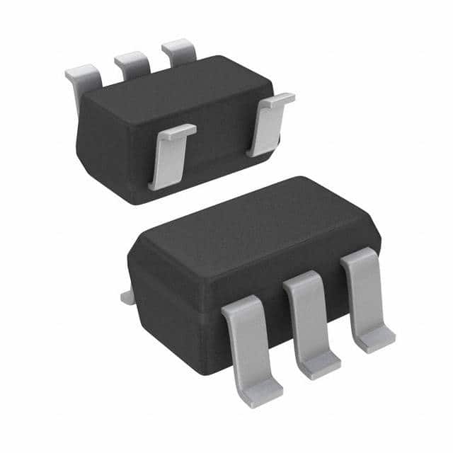
Xem thông số kỹ thuật để biết chi tiết sản phẩm.

TL331IDBVTE4
Basic Information Overview
- Category: Integrated Circuit (IC)
- Use: Voltage Comparator
- Characteristics: Low-power, high-speed, precision comparator
- Package: SOT-23-5
- Essence: TL331IDBVTE4 is a voltage comparator IC designed for low-power applications that require high-speed and precision.
- Packaging/Quantity: Available in tape and reel packaging with 3000 units per reel.
Specifications
- Supply Voltage Range: 2 V to 36 V
- Input Offset Voltage: ±1 mV
- Response Time: 3.5 µs
- Operating Temperature Range: -40°C to +125°C
- Output Current: 50 mA
- Quiescent Current: 60 µA
Detailed Pin Configuration
The TL331IDBVTE4 IC has the following pin configuration: 1. Non-Inverting Input (IN+) 2. Inverting Input (IN-) 3. Output (OUT) 4. Ground (GND) 5. Supply Voltage (VCC)
Functional Features
- High-speed operation: The TL331IDBVTE4 offers fast response time of 3.5 µs, making it suitable for time-critical applications.
- Low-power consumption: With a quiescent current of only 60 µA, this IC is ideal for battery-powered devices.
- Wide supply voltage range: The TL331IDBVTE4 can operate from 2 V to 36 V, providing flexibility in various voltage environments.
- Precision performance: It has a low input offset voltage of ±1 mV, ensuring accurate comparison of input voltages.
Advantages and Disadvantages
Advantages: - High-speed operation - Low-power consumption - Wide supply voltage range - Precision performance
Disadvantages: - Limited output current capacity (50 mA) - Limited temperature range (-40°C to +125°C)
Working Principles
The TL331IDBVTE4 is a voltage comparator that compares the voltages at its non-inverting and inverting inputs. It amplifies the voltage difference between these inputs and produces a digital output signal based on the comparison result. The output is high when the non-inverting input voltage is greater than the inverting input voltage, and low otherwise.
Detailed Application Field Plans
The TL331IDBVTE4 is commonly used in various applications, including: 1. Battery-powered devices: Its low-power consumption makes it suitable for portable electronics such as smartphones, tablets, and wearables. 2. Industrial automation: It can be used in control systems, motor drives, and power management circuits. 3. Automotive electronics: The IC finds applications in automotive systems like engine control units, lighting control, and battery monitoring. 4. Communication equipment: It is utilized in telecom infrastructure, networking devices, and data communication systems.
Detailed and Complete Alternative Models
- LM339: A quad voltage comparator with similar characteristics and pin configuration.
- LM311: A high-speed voltage comparator with differential inputs and adjustable hysteresis.
- LM393: A dual voltage comparator with low-power consumption and wide supply voltage range.
These alternative models offer similar functionality and can be considered as substitutes for the TL331IDBVTE4 in different applications.
Word count: 386 words
Liệt kê 10 câu hỏi và câu trả lời thường gặp liên quan đến ứng dụng TL331IDBVTE4 trong giải pháp kỹ thuật
Sure! Here are 10 common questions and answers related to the application of TL331IDBVTE4 in technical solutions:
Q: What is TL331IDBVTE4? A: TL331IDBVTE4 is a precision voltage comparator integrated circuit (IC) commonly used in technical solutions.
Q: What is the operating voltage range of TL331IDBVTE4? A: The operating voltage range of TL331IDBVTE4 is typically between 2V and 36V.
Q: What is the output type of TL331IDBVTE4? A: TL331IDBVTE4 has an open-drain output, which means it can sink current but cannot source current.
Q: What is the typical response time of TL331IDBVTE4? A: The typical response time of TL331IDBVTE4 is around 1.3 microseconds.
Q: Can TL331IDBVTE4 operate in both single-supply and dual-supply configurations? A: Yes, TL331IDBVTE4 can operate in both single-supply and dual-supply configurations.
Q: What is the input offset voltage of TL331IDBVTE4? A: The input offset voltage of TL331IDBVTE4 is typically around 2mV.
Q: Is TL331IDBVTE4 suitable for low-power applications? A: Yes, TL331IDBVTE4 is designed for low-power applications and has a low quiescent current consumption.
Q: Can TL331IDBVTE4 tolerate high temperatures? A: Yes, TL331IDBVTE4 has a wide temperature range and can operate reliably at high temperatures up to 125°C.
Q: What is the input common-mode voltage range of TL331IDBVTE4? A: The input common-mode voltage range of TL331IDBVTE4 is typically between -0.3V and VCC+0.3V.
Q: Can TL331IDBVTE4 be used in automotive applications? A: Yes, TL331IDBVTE4 is qualified for automotive applications and meets the necessary standards and requirements.
Please note that the answers provided here are general and may vary depending on specific datasheet specifications and application requirements.

