

Xem thông số kỹ thuật để biết chi tiết sản phẩm.
TLV3702CDGKR
Product Overview
- Category: Integrated Circuits (ICs)
- Use: Comparator
- Characteristics: High-speed, low-power, rail-to-rail input/output, open-drain output, wide supply voltage range
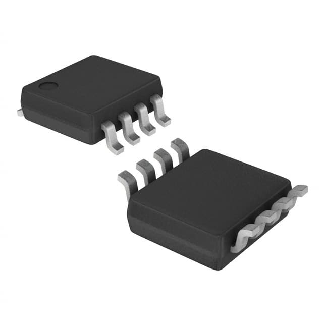
- Package: 8-VSSOP (0.091", 2.30mm Width)
- Essence: TLV3702CDGKR is a dual-channel, high-speed comparator designed for various applications requiring precision signal detection and comparison.
- Packaging/Quantity: Tape & Reel (3000 pieces per reel)
Specifications
- Supply Voltage Range: 2.7V to 16V
- Input Offset Voltage: ±1mV (maximum)
- Input Bias Current: ±10nA (maximum)
- Response Time: 5ns (typical)
- Operating Temperature Range: -40°C to +125°C
Detailed Pin Configuration
The TLV3702CDGKR has the following pin configuration:
```
| | --|IN+ IN-|-- Non-inverting and inverting inputs --|VCC GND|-- Power supply pins --|OUT |-- Output pin |___________| ```
Functional Features
- High-speed operation allows for quick response time in signal detection.
- Low-power consumption makes it suitable for battery-powered applications.
- Rail-to-rail input/output capability enables accurate signal detection across the entire supply voltage range.
- Open-drain output provides flexibility in interfacing with other devices.
- Wide supply voltage range allows for compatibility with various power sources.
Advantages and Disadvantages
Advantages: - High-speed operation ensures fast response time. - Low-power consumption extends battery life. - Rail-to-rail input/output capability enables accurate signal detection. - Open-drain output provides flexibility in circuit design. - Wide supply voltage range allows for versatile applications.
Disadvantages: - Limited number of channels (dual-channel only). - May not be suitable for applications requiring high precision due to input offset voltage.
Working Principles
The TLV3702CDGKR operates as a voltage comparator, comparing the voltages at its non-inverting and inverting inputs. When the voltage at the non-inverting input is higher than the voltage at the inverting input, the output goes low (0V). Conversely, when the voltage at the inverting input is higher, the output goes high (VCC).
Detailed Application Field Plans
The TLV3702CDGKR can be used in various applications, including but not limited to:
- Battery-powered devices: Due to its low-power consumption, it is suitable for portable electronics such as handheld meters, medical devices, and remote sensors.
- Motor control systems: The high-speed operation makes it ideal for detecting motor position and controlling motor speed.
- Signal conditioning circuits: It can be used in analog-to-digital converters (ADCs) and digital-to-analog converters (DACs) for precise signal detection and conversion.
- Overvoltage/undervoltage protection: The comparator can be utilized to monitor power supply voltages and trigger protective measures when they exceed or fall below certain thresholds.
Detailed and Complete Alternative Models
Some alternative models that offer similar functionality to the TLV3702CDGKR include:
- LM393: Dual voltage comparator with open-drain outputs.
- MAX9117: High-speed, low-power comparator with rail-to-rail inputs and push-pull outputs.
- LT1716: Precision comparator with low input offset voltage and wide supply voltage range.
These alternatives can be considered based on specific application requirements and design constraints.
Word count: 455 words
Liệt kê 10 câu hỏi và câu trả lời thường gặp liên quan đến ứng dụng TLV3702CDGKR trong giải pháp kỹ thuật
Sure! Here are 10 common questions and answers related to the application of TLV3702CDGKR in technical solutions:
Q: What is TLV3702CDGKR? A: TLV3702CDGKR is a dual-channel, high-precision voltage comparator IC.
Q: What is the supply voltage range for TLV3702CDGKR? A: The supply voltage range for TLV3702CDGKR is typically between 2.7V and 16V.
Q: What is the input voltage range for TLV3702CDGKR? A: The input voltage range for TLV3702CDGKR is typically between -0.1V and Vcc + 0.1V.
Q: What is the output voltage range for TLV3702CDGKR? A: The output voltage range for TLV3702CDGKR is typically between GND and Vcc.
Q: What is the typical response time of TLV3702CDGKR? A: The typical response time of TLV3702CDGKR is around 1.3µs.
Q: Can TLV3702CDGKR operate in both single-supply and dual-supply configurations? A: Yes, TLV3702CDGKR can operate in both single-supply and dual-supply configurations.
Q: What is the maximum operating temperature range for TLV3702CDGKR? A: The maximum operating temperature range for TLV3702CDGKR is typically between -40°C and 125°C.
Q: Does TLV3702CDGKR have built-in hysteresis? A: Yes, TLV3702CDGKR has built-in hysteresis to prevent output oscillation near the threshold voltage.
Q: Can TLV3702CDGKR be used in automotive applications? A: Yes, TLV3702CDGKR is qualified for automotive applications and meets AEC-Q100 standards.
Q: What are some typical applications of TLV3702CDGKR? A: TLV3702CDGKR is commonly used in battery-powered systems, motor control, level detection, and general-purpose comparator circuits.
Please note that the answers provided here are general and may vary depending on specific datasheet specifications and application requirements.