

Xem thông số kỹ thuật để biết chi tiết sản phẩm.
TPS22930AYZVR
Product Overview
Category
The TPS22930AYZVR belongs to the category of power management integrated circuits (PMICs).
Use
It is primarily used for managing power in electronic devices, specifically for load switching applications.
Characteristics
- Low on-resistance
- Fast switching speed
- Low quiescent current
- Overcurrent and thermal protection
- Wide input voltage range
Package
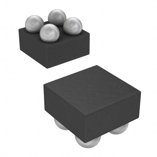
The TPS22930AYZVR comes in a small 4-ball wafer chip scale package (WCSP), measuring 0.8mm x 0.8mm.
Essence
The essence of the TPS22930AYZVR lies in its ability to efficiently control power flow in electronic devices, ensuring optimal performance and protection.
Packaging/Quantity
The TPS22930AYZVR is typically packaged in reels, with 3000 units per reel.
Specifications
- Input Voltage Range: 1.5V to 5.5V
- On-Resistance: 20mΩ (typical)
- Quiescent Current: 0.5µA (typical)
- Maximum Continuous Current: 2A
- Operating Temperature Range: -40°C to +85°C
Detailed Pin Configuration
The TPS22930AYZVR has the following pin configuration:
- VIN: Input voltage pin
- GND: Ground pin
- EN: Enable pin
- VOUT: Output voltage pin
Functional Features
- Load switching capability
- Power sequencing support
- Overcurrent protection
- Thermal shutdown protection
- Low power consumption in standby mode
Advantages and Disadvantages
Advantages
- Low on-resistance ensures minimal power loss
- Fast switching speed improves overall system efficiency
- Wide input voltage range allows for versatile applications
- Overcurrent and thermal protection enhance device safety
Disadvantages
- Limited maximum continuous current may restrict usage in high-power applications
- Small package size may require careful handling during assembly
Working Principles
The TPS22930AYZVR operates by controlling the flow of power from the input voltage (VIN) to the output voltage (VOUT) based on the enable (EN) pin. When the EN pin is high, the device allows power to flow from VIN to VOUT. Conversely, when the EN pin is low, the device cuts off the power flow.
Detailed Application Field Plans
The TPS22930AYZVR finds application in various electronic devices that require efficient load switching and power management. Some potential application fields include:
- Mobile devices: Smartphones, tablets, and wearables can benefit from the TPS22930AYZVR's low power consumption and fast switching speed.
- Portable gaming consoles: The device's overcurrent and thermal protection features make it suitable for managing power in gaming devices.
- IoT devices: Internet of Things (IoT) devices often have strict power requirements, making the TPS22930AYZVR an ideal choice for power management in these applications.
Detailed and Complete Alternative Models
- TPS22931AYZVR: Similar to the TPS22930AYZVR, but with a higher maximum continuous current of 3A.
- TPS22932AYZVR: A variant with a lower on-resistance of 10mΩ, allowing for even lower power loss.
- TPS22933AYZVR: Offers a wider input voltage range of 1.0V to 5.5V, providing more flexibility in power supply options.
These alternative models provide similar functionality to the TPS22930AYZVR but offer different specifications to suit specific application requirements.
In conclusion, the TPS22930AYZVR is a power management integrated circuit that excels in load switching applications. With its low on-resistance, fast switching speed, and comprehensive protection features, it offers efficient power management for various electronic devices. Its small package size and wide input voltage range make it suitable for diverse applications. However, its limited maximum continuous current and small package size should be considered when selecting alternative models for high-power applications or specific assembly requirements.
Liệt kê 10 câu hỏi và câu trả lời thường gặp liên quan đến ứng dụng TPS22930AYZVR trong giải pháp kỹ thuật
What is the input voltage range of TPS22930AYZVR?
- The input voltage range of TPS22930AYZVR is 0V to 5.5V.What is the maximum continuous current that TPS22930AYZVR can handle?
- TPS22930AYZVR can handle a maximum continuous current of 3A.Can TPS22930AYZVR be used for power sequencing applications?
- Yes, TPS22930AYZVR is suitable for power sequencing applications.What is the typical on-state resistance of TPS22930AYZVR?
- The typical on-state resistance of TPS22930AYZVR is 20mΩ.Is TPS22930AYZVR compatible with both analog and digital signals?
- Yes, TPS22930AYZVR is compatible with both analog and digital signals.Does TPS22930AYZVR have built-in thermal shutdown protection?
- Yes, TPS22930AYZVR features built-in thermal shutdown protection.Can TPS22930AYZVR be used in battery-powered applications?
- Yes, TPS22930AYZVR is suitable for battery-powered applications.What is the operating temperature range of TPS22930AYZVR?
- The operating temperature range of TPS22930AYZVR is -40°C to 85°C.Is TPS22930AYZVR available in a small package for space-constrained designs?
- Yes, TPS22930AYZVR is available in a small 1.5mm x 1.5mm package.Can TPS22930AYZVR be used in automotive electronics applications?
- Yes, TPS22930AYZVR is suitable for use in automotive electronics applications.