

Xem thông số kỹ thuật để biết chi tiết sản phẩm.
XC6118N11DGR-G
Product Overview
Category
XC6118N11DGR-G belongs to the category of voltage regulators.
Use
It is commonly used in electronic circuits to regulate and stabilize voltage levels.
Characteristics
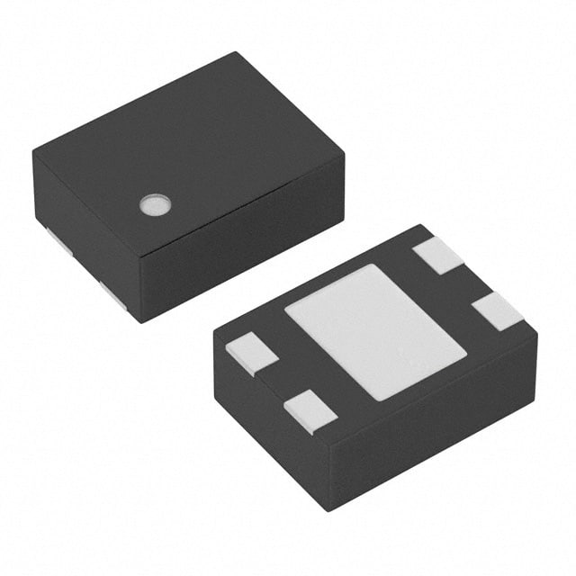
- Package: DFN (Dual Flat No-Lead)
- Essence: Low Dropout Voltage Regulator
- Packaging/Quantity: Tape & Reel, 3000 pieces per reel
Specifications
The specifications for XC6118N11DGR-G are as follows:
- Input Voltage Range: 2.5V to 6.0V
- Output Voltage: 1.1V
- Output Current: 150mA
- Dropout Voltage: 200mV (typical)
- Quiescent Current: 30µA (typical)
- Operating Temperature Range: -40°C to +85°C
Detailed Pin Configuration
XC6118N11DGR-G has the following pin configuration:
- VIN (Input Voltage)
- GND (Ground)
- VOUT (Output Voltage)
Functional Features
The functional features of XC6118N11DGR-G include:
- Low dropout voltage for efficient regulation
- Low quiescent current for power-saving operation
- Overcurrent protection to prevent damage
- Thermal shutdown protection for temperature control
- Short-circuit protection for circuit safety
Advantages and Disadvantages
Advantages: - Low dropout voltage ensures efficient voltage regulation - Low quiescent current minimizes power consumption - Overcurrent, thermal shutdown, and short-circuit protections enhance reliability
Disadvantages: - Limited output current capacity (150mA)
Working Principles
XC6118N11DGR-G works by regulating the input voltage to a stable output voltage of 1.1V. It achieves this through a combination of internal circuitry and feedback control mechanisms. The low dropout voltage ensures efficient regulation even when the input voltage is close to the desired output voltage.
Detailed Application Field Plans
XC6118N11DGR-G finds applications in various electronic devices and systems, including but not limited to:
- Mobile phones
- Tablets
- Portable media players
- Wearable devices
- IoT (Internet of Things) devices
- Battery-powered devices
Detailed and Complete Alternative Models
Some alternative models that can be considered as alternatives to XC6118N11DGR-G are:
- XC6206P332MR-G: 3.3V Low Dropout Voltage Regulator
- XC6220B331MR-G: 3.3V Ultra-Low Quiescent Current LDO Regulator
- XC6219B331MR-G: 3.3V High-Speed LDO Regulator with Enable Function
- XC6221B331MR-G: 3.3V High-Speed LDO Regulator with Power-On Reset
These alternative models offer different features and specifications, allowing users to choose the most suitable option for their specific requirements.
In conclusion, XC6118N11DGR-G is a voltage regulator with low dropout voltage, making it ideal for various electronic applications. Its compact package, low quiescent current, and built-in protections contribute to its reliability and efficiency.
Liệt kê 10 câu hỏi và câu trả lời thường gặp liên quan đến ứng dụng XC6118N11DGR-G trong giải pháp kỹ thuật
Sure! Here are 10 common questions and answers related to the application of XC6118N11DGR-G in technical solutions:
Question: What is XC6118N11DGR-G?
Answer: XC6118N11DGR-G is a voltage detector IC (integrated circuit) that monitors the power supply voltage and provides a reset signal when the voltage drops below a certain threshold.Question: What is the operating voltage range of XC6118N11DGR-G?
Answer: The operating voltage range of XC6118N11DGR-G is typically between 0.9V and 6.0V.Question: How does XC6118N11DGR-G help in technical solutions?
Answer: XC6118N11DGR-G helps in technical solutions by providing a reliable reset signal to microcontrollers, DSPs, or other digital devices when the power supply voltage falls below a specified level, ensuring proper system initialization.Question: Can XC6118N11DGR-G be used in battery-powered applications?
Answer: Yes, XC6118N11DGR-G can be used in battery-powered applications as it has a low quiescent current consumption of typically 1.0µA, making it suitable for power-sensitive designs.Question: What is the output type of XC6118N11DGR-G?
Answer: XC6118N11DGR-G has an open-drain output type, which allows for flexibility in connecting to different microcontrollers or devices.Question: What is the typical reset threshold voltage of XC6118N11DGR-G?
Answer: The typical reset threshold voltage of XC6118N11DGR-G is 1.1V.Question: Does XC6118N11DGR-G have a built-in delay time?
Answer: Yes, XC6118N11DGR-G has a built-in delay time of typically 200ms to prevent false reset signals during power supply fluctuations.Question: Can XC6118N11DGR-G be used in automotive applications?
Answer: Yes, XC6118N11DGR-G is AEC-Q100 qualified and can be used in automotive applications where reliable voltage monitoring and system initialization are required.Question: What is the temperature range for XC6118N11DGR-G?
Answer: The temperature range for XC6118N11DGR-G is typically -40°C to +85°C, making it suitable for a wide range of operating conditions.Question: Is XC6118N11DGR-G available in different package options?
Answer: Yes, XC6118N11DGR-G is available in various package options, including SOT-25 and USP-4B, providing flexibility for different PCB layouts and space constraints.
Please note that the answers provided here are general and may vary depending on the specific datasheet and manufacturer's specifications for XC6118N11DGR-G.