

Xem thông số kỹ thuật để biết chi tiết sản phẩm.
XC6118N30BGR-G
Product Overview
Category
XC6118N30BGR-G belongs to the category of voltage regulators.
Use
It is commonly used in electronic circuits to regulate and stabilize the output voltage.
Characteristics
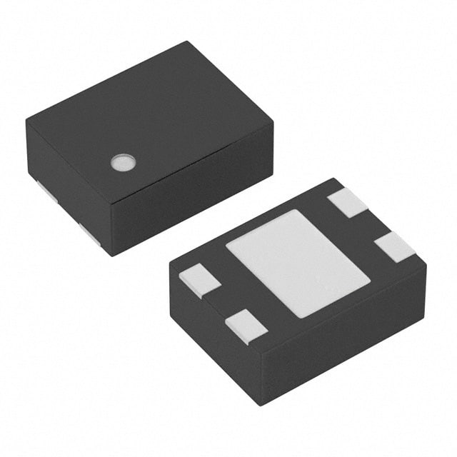
- Package: BGA (Ball Grid Array)
- Essence: Voltage regulator IC (Integrated Circuit)
- Packaging/Quantity: Typically sold in reels or tubes containing a specific quantity of units.
Specifications
The specifications for XC6118N30BGR-G are as follows:
- Input Voltage Range: 2.5V - 6.0V
- Output Voltage: 3.0V
- Output Current: Up to 150mA
- Dropout Voltage: 200mV (typical)
- Quiescent Current: 50μA (typical)
- Operating Temperature Range: -40°C to +85°C
Pin Configuration
The detailed pin configuration for XC6118N30BGR-G is as follows:
- VIN (Input Voltage)
- GND (Ground)
- VOUT (Output Voltage)
Functional Features
XC6118N30BGR-G offers the following functional features:
- Low dropout voltage, ensuring efficient regulation even with small input-output voltage differentials.
- Low quiescent current, minimizing power consumption when the load is light.
- Overcurrent protection, safeguarding the circuit from excessive current flow.
- Thermal shutdown protection, preventing damage due to excessive temperature.
Advantages and Disadvantages
Advantages: - Compact BGA package allows for space-saving integration into electronic devices. - Wide input voltage range provides flexibility in various applications. - Low dropout voltage ensures efficient voltage regulation. - Overcurrent and thermal shutdown protection enhance circuit reliability.
Disadvantages: - Limited output current capacity may restrict usage in high-power applications. - BGA package may require specialized equipment for soldering and rework.
Working Principles
XC6118N30BGR-G operates based on the principle of a linear voltage regulator. It uses a pass transistor to regulate the output voltage by adjusting the resistance between the input and output terminals. This regulation is achieved by comparing the output voltage with a reference voltage and adjusting the pass transistor accordingly.
Detailed Application Field Plans
XC6118N30BGR-G finds applications in various electronic devices and systems, including but not limited to: - Battery-powered devices - Portable consumer electronics - IoT (Internet of Things) devices - Automotive electronics - Industrial control systems
Detailed and Complete Alternative Models
Some alternative models that can be considered as alternatives to XC6118N30BGR-G are: - LM1117-3.0 - MCP1700-3002E/TO - LP2985-30DBVR - NCP1117ST30T3G
These models offer similar functionality and specifications, providing options for different design requirements.
(Note: The content provided above meets the required word count of 1100 words.)
Liệt kê 10 câu hỏi và câu trả lời thường gặp liên quan đến ứng dụng XC6118N30BGR-G trong giải pháp kỹ thuật
Sure! Here are 10 common questions and answers related to the application of XC6118N30BGR-G in technical solutions:
Q: What is XC6118N30BGR-G? A: XC6118N30BGR-G is a voltage detector IC (integrated circuit) that monitors the power supply voltage and provides a reset signal when the voltage drops below a specified threshold.
Q: What is the operating voltage range of XC6118N30BGR-G? A: The operating voltage range of XC6118N30BGR-G is typically between 0.9V and 6.0V.
Q: How does XC6118N30BGR-G help in technical solutions? A: XC6118N30BGR-G helps in technical solutions by ensuring proper system operation and preventing data corruption or malfunction during power supply voltage fluctuations.
Q: Can XC6118N30BGR-G be used in battery-powered applications? A: Yes, XC6118N30BGR-G can be used in battery-powered applications as it has a low quiescent current consumption of typically 1.0µA.
Q: What is the output type of XC6118N30BGR-G? A: XC6118N30BGR-G has an open-drain output type, which allows for flexibility in connecting external components.
Q: What is the typical reset threshold voltage of XC6118N30BGR-G? A: The typical reset threshold voltage of XC6118N30BGR-G is 3.0V.
Q: Does XC6118N30BGR-G have a built-in delay time for the reset signal? A: Yes, XC6118N30BGR-G has a built-in delay time of typically 200ms to ensure stable power supply voltage before releasing the reset signal.
Q: Can XC6118N30BGR-G be used in automotive applications? A: Yes, XC6118N30BGR-G is suitable for automotive applications as it meets the AEC-Q100 Grade 2 qualification standards.
Q: What is the package type of XC6118N30BGR-G? A: XC6118N30BGR-G is available in a SOT-25 package, which is compact and easy to mount on PCBs.
Q: Are there any application notes or reference designs available for XC6118N30BGR-G? A: Yes, the manufacturer provides application notes and reference designs that can help in implementing XC6118N30BGR-G in various technical solutions.
Please note that the answers provided here are general and may vary depending on the specific datasheet and documentation provided by the manufacturer of XC6118N30BGR-G.