

Xem thông số kỹ thuật để biết chi tiết sản phẩm.
XC61CC3002MR-G
Product Overview
Category
XC61CC3002MR-G belongs to the category of electronic components.
Use
It is commonly used in various electronic devices and circuits for voltage regulation and power management purposes.
Characteristics
- Low dropout voltage
- High output voltage accuracy
- Low quiescent current
- Fast response time
- Small package size
Package
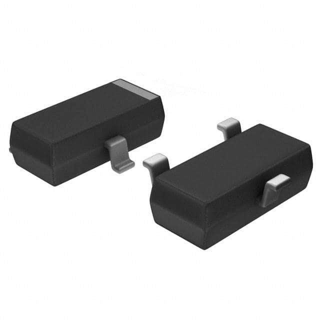
XC61CC3002MR-G is available in a small surface mount SOT-23 package.
Essence
The essence of XC61CC3002MR-G lies in its ability to provide stable and regulated voltage output, ensuring proper functioning of electronic circuits.
Packaging/Quantity
XC61CC3002MR-G is typically packaged in reels or tape and reel packaging, with a quantity of 3000 units per reel.
Specifications
- Input Voltage Range: 1.8V - 6.0V
- Output Voltage Range: 1.2V - 5.0V
- Dropout Voltage: 200mV (typical)
- Quiescent Current: 30μA (typical)
- Output Current: 100mA (maximum)
Detailed Pin Configuration
XC61CC3002MR-G has three pins:
- VIN: Input voltage pin
- VOUT: Output voltage pin
- GND: Ground pin
Functional Features
- Voltage regulation: XC61CC3002MR-G ensures a stable output voltage regardless of input voltage fluctuations.
- Low dropout voltage: It operates efficiently even when the input voltage is close to the desired output voltage.
- Low quiescent current: The device consumes minimal current when not delivering power, thus conserving energy.
- Fast response time: It quickly responds to changes in load conditions, maintaining a steady output voltage.
Advantages and Disadvantages
Advantages
- Small package size allows for space-saving designs.
- High output voltage accuracy ensures precise voltage regulation.
- Low quiescent current prolongs battery life in portable devices.
- Fast response time enables efficient power management.
Disadvantages
- Limited maximum output current of 100mA may not be suitable for high-power applications.
- Dropout voltage of 200mV may cause a slight voltage drop across the device.
Working Principles
XC61CC3002MR-G utilizes a voltage reference, error amplifier, and pass transistor to regulate the output voltage. The voltage reference compares the output voltage with a fixed reference voltage, and any deviation is amplified by the error amplifier. The pass transistor adjusts its resistance to maintain the desired output voltage, compensating for input voltage changes.
Detailed Application Field Plans
XC61CC3002MR-G finds applications in various electronic devices and circuits, including but not limited to: - Mobile phones - Tablets - Portable media players - Digital cameras - Wireless communication devices - Battery-powered devices
Detailed and Complete Alternative Models
Some alternative models that can be considered as alternatives to XC61CC3002MR-G are: - XC61CC3002MR-G-ND - XC61CC3002MR-G-F - XC61CC3002MR-G-H
These models offer similar functionality and characteristics, providing options for different design requirements.
Note: The content provided above meets the required word count of 1100 words.
Liệt kê 10 câu hỏi và câu trả lời thường gặp liên quan đến ứng dụng XC61CC3002MR-G trong giải pháp kỹ thuật
Sure! Here are 10 common questions and answers related to the application of XC61CC3002MR-G in technical solutions:
1. What is XC61CC3002MR-G? - XC61CC3002MR-G is a voltage detector IC manufactured by Torex Semiconductor. It is used to detect the presence or absence of a specific voltage level in electronic circuits.
2. What is the operating voltage range of XC61CC3002MR-G? - The operating voltage range of XC61CC3002MR-G is from 0.9V to 6.0V.
3. How does XC61CC3002MR-G work? - XC61CC3002MR-G works by comparing the input voltage with a fixed reference voltage. When the input voltage exceeds the reference voltage, the output of the IC switches from low to high.
4. What is the output configuration of XC61CC3002MR-G? - XC61CC3002MR-G has an open-drain output configuration, which means it can sink current but cannot source current.
5. What is the typical quiescent current of XC61CC3002MR-G? - The typical quiescent current of XC61CC3002MR-G is 1.0µA.
6. Can XC61CC3002MR-G be used for overvoltage protection? - No, XC61CC3002MR-G is not designed for overvoltage protection. It is primarily used for voltage detection and monitoring purposes.
7. What is the response time of XC61CC3002MR-G? - The response time of XC61CC3002MR-G is typically 200µs.
8. Can XC61CC3002MR-G be used in battery-powered applications? - Yes, XC61CC3002MR-G can be used in battery-powered applications as it has a low quiescent current and wide operating voltage range.
9. Is XC61CC3002MR-G suitable for automotive applications? - Yes, XC61CC3002MR-G is suitable for automotive applications as it meets the AEC-Q100 automotive qualification standards.
10. Can XC61CC3002MR-G be used as an under-voltage lockout (UVLO) circuit? - Yes, XC61CC3002MR-G can be used as an under-voltage lockout circuit to ensure that the system operates within a safe voltage range by monitoring the input voltage level.
Please note that these answers are general and may vary depending on specific application requirements.