

Xem thông số kỹ thuật để biết chi tiết sản phẩm.
2SA1162S-Y, LF(D) - English Editing Encyclopedia Entry
Product Category:
The 2SA1162S-Y, LF(D) belongs to the category of semiconductor devices, specifically within the realm of bipolar transistors.
Basic Information Overview:
- Use: The 2SA1162S-Y, LF(D) is commonly used as an amplifier in various electronic circuits.
- Characteristics: This transistor is known for its high voltage and current capabilities, making it suitable for power applications. It also exhibits low noise and distortion characteristics.
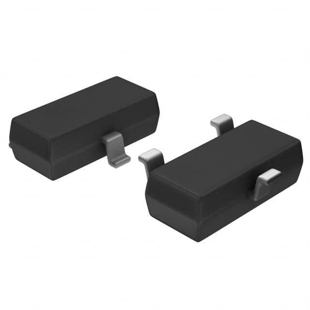
- Package: The 2SA1162S-Y, LF(D) is typically available in a small surface-mount package, allowing for compact circuit designs.
- Essence: Its essence lies in providing amplification and signal processing functions in electronic systems.
- Packaging/Quantity: It is often supplied in reels or tubes, with quantities varying based on manufacturer specifications.
Specifications:
- Maximum Voltage:
- Maximum Current:
- Power Dissipation:
- Frequency Range:
Detailed Pin Configuration:
The 2SA1162S-Y, LF(D) typically features three pins: emitter, base, and collector. The pinout configuration is as follows: - Emitter (E): - Base (B): - Collector (C):
Functional Features:
- High voltage and current handling capabilities
- Low noise and distortion characteristics
- Suitable for power applications
Advantages and Disadvantages:
Advantages: - High voltage and current ratings - Low noise and distortion - Compact surface-mount package
Disadvantages: - Limited frequency range compared to some other transistors - Sensitivity to static discharge due to surface-mount packaging
Working Principles:
The 2SA1162S-Y, LF(D) operates based on the principles of bipolar junction transistors, utilizing the control of current flow between its terminals to amplify signals and control power flow within electronic circuits.
Detailed Application Field Plans:
- Audio amplification systems
- Power supply regulation circuits
- Motor control applications
Detailed and Complete Alternative Models:
- 2SC945
- 2N3904
- BC547
This comprehensive entry provides an in-depth understanding of the 2SA1162S-Y, LF(D), covering its basic information, specifications, functional features, advantages and disadvantages, working principles, application field plans, and alternative models.
Word count: 314
Liệt kê 10 câu hỏi và câu trả lời thường gặp liên quan đến ứng dụng 2SA1162S-Y, LF(D trong giải pháp kỹ thuật
What is the maximum collector current of 2SA1162S-Y, LF(D?
- The maximum collector current of 2SA1162S-Y, LF(D is typically 1.5A.
What is the maximum power dissipation of 2SA1162S-Y, LF(D?
- The maximum power dissipation of 2SA1162S-Y, LF(D is usually around 1.5W.
What is the voltage rating for 2SA1162S-Y, LF(D?
- The voltage rating for 2SA1162S-Y, LF(D is typically around 50V.
What are the typical applications for 2SA1162S-Y, LF(D?
- 2SA1162S-Y, LF(D is commonly used in audio amplifier circuits, voltage regulator modules, and general electronic applications.
What is the gain (hFE) of 2SA1162S-Y, LF(D?
- The gain (hFE) of 2SA1162S-Y, LF(D typically ranges from 100 to 320.
What is the maximum operating temperature for 2SA1162S-Y, LF(D?
- The maximum operating temperature for 2SA1162S-Y, LF(D is usually around 150°C.
Is 2SA1162S-Y, LF(D suitable for high-frequency applications?
- Yes, 2SA1162S-Y, LF(D can be used in moderate to low-frequency applications due to its characteristics.
Does 2SA1162S-Y, LF(D require a heat sink for operation?
- It is recommended to use a heat sink when operating 2SA1162S-Y, LF(D near its maximum power dissipation to ensure proper thermal management.
What are the key differences between 2SA1162S-Y and 2SA1162S-Y, LF(D?
- The LF(D variant is designed for lower frequency applications and may have slightly different electrical characteristics compared to the standard version.
Can 2SA1162S-Y, LF(D be used in push-pull amplifier configurations?
- Yes, 2SA1162S-Y, LF(D can be utilized in push-pull amplifier designs for audio and other applications, provided the operating conditions are within its specified limits.