

Xem thông số kỹ thuật để biết chi tiết sản phẩm.
TC7W04FU(TE12L)
Basic Information Overview
- Category: Integrated Circuit (IC)
- Use: Logic Gate
- Characteristics: Dual Inverter
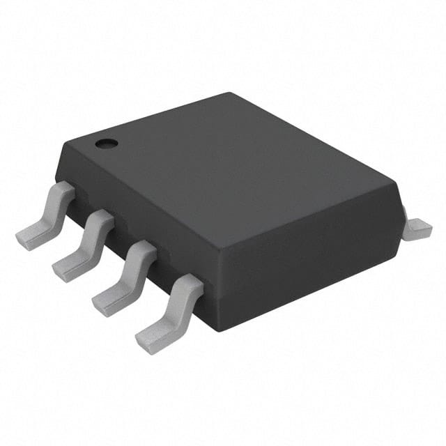
- Package: SOT-353
- Essence: High-Speed CMOS Logic
- Packaging/Quantity: Tape and Reel, 3000 pieces per reel
Specifications
- Supply Voltage: 1.65V to 5.5V
- Input Voltage: 0V to VCC
- Output Voltage: 0V to VCC
- Operating Temperature Range: -40°C to +85°C
- Propagation Delay Time: 3.4ns (typical) at VCC = 3.3V, CL = 15pF
Detailed Pin Configuration
The TC7W04FU(TE12L) has a total of 5 pins:
- GND (Ground): Connected to the ground reference potential.
- A (Input A): Input pin for the first inverter.
- Y (Output Y): Output pin for the first inverter.
- B (Input B): Input pin for the second inverter.
- Z (Output Z): Output pin for the second inverter.
Functional Features
- Dual Inverter: The TC7W04FU(TE12L) consists of two independent inverters in a single package.
- High-Speed Operation: It operates at high speeds, making it suitable for applications requiring fast switching.
- Wide Voltage Range: The IC can be powered by a supply voltage ranging from 1.65V to 5.5V, providing flexibility in various applications.
- Low Power Consumption: The IC is designed to consume low power, making it energy-efficient.
Advantages and Disadvantages
Advantages: - Compact Size: The SOT-353 package allows for space-saving and integration in small electronic devices. - High-Speed Performance: The IC offers fast propagation delay times, enabling quick signal processing. - Versatile Voltage Range: It can operate with a wide range of supply voltages, enhancing compatibility with different systems.
Disadvantages: - Limited Functionality: As a dual inverter, it has a specific function and may not be suitable for complex logic operations. - Sensitivity to Noise: High-speed operation makes the IC more susceptible to noise interference, requiring proper noise mitigation measures.
Working Principles
The TC7W04FU(TE12L) is based on high-speed CMOS technology. Each inverter within the IC consists of complementary metal-oxide-semiconductor (CMOS) transistors. When an input signal is applied, the transistors switch states, resulting in an inverted output signal. The dual inverter configuration allows for signal amplification or inversion as required by the application.
Detailed Application Field Plans
The TC7W04FU(TE12L) finds applications in various fields, including:
- Digital Electronics: It can be used in digital circuits for signal inversion, level shifting, and buffering.
- Communication Systems: The IC is suitable for use in communication systems, such as data transmission and reception modules.
- Microcontrollers: It can be integrated into microcontroller-based systems for signal conditioning and interfacing.
- Consumer Electronics: The IC can be utilized in devices like smartphones, tablets, and gaming consoles for signal processing and control.
Detailed and Complete Alternative Models
- SN74LVC2G04: Dual Inverter Gate, SOT-353 package, operating voltage range of 1.65V to 5.5V.
- MC74VHC1G04: Single Inverter Gate, SOT-353 package, operating voltage range of 2V to 6V.
- CD4049UB: Hex Inverting Buffer/Converter, DIP-16 package, operating voltage range of 3V to 18V.
These alternative models offer similar functionality and can be considered as substitutes for the TC7W04FU(TE12L) based on specific application requirements.
Word count: 383 words
Liệt kê 10 câu hỏi và câu trả lời thường gặp liên quan đến ứng dụng TC7W04FU(TE12L) trong giải pháp kỹ thuật
Sure! Here are 10 common questions and answers related to the application of TC7W04FU(TE12L) in technical solutions:
Question: What is TC7W04FU(TE12L)?
Answer: TC7W04FU(TE12L) is a specific model number for a logic gate IC (integrated circuit) manufactured by Toshiba.Question: What is the function of TC7W04FU(TE12L)?
Answer: TC7W04FU(TE12L) is a hex inverter gate, which means it can invert the input signal and provide the complementary output.Question: What voltage levels does TC7W04FU(TE12L) support?
Answer: TC7W04FU(TE12L) supports a wide range of voltage levels, typically from 2V to 6V.Question: Can TC7W04FU(TE12L) be used in both digital and analog circuits?
Answer: No, TC7W04FU(TE12L) is specifically designed for digital circuits and is not suitable for analog applications.Question: How many inputs and outputs does TC7W04FU(TE12L) have?
Answer: TC7W04FU(TE12L) has six inputs and six outputs, as it is a hex inverter gate.Question: What is the maximum operating frequency of TC7W04FU(TE12L)?
Answer: The maximum operating frequency of TC7W04FU(TE12L) is typically around 100 MHz.Question: Can TC7W04FU(TE12L) be used in high-temperature environments?
Answer: Yes, TC7W04FU(TE12L) has a wide operating temperature range and can be used in high-temperature environments up to 125°C.Question: Is TC7W04FU(TE12L) compatible with other logic families?
Answer: Yes, TC7W04FU(TE12L) is compatible with various logic families such as TTL (Transistor-Transistor Logic) and CMOS (Complementary Metal-Oxide-Semiconductor).Question: Can TC7W04FU(TE12L) be used for level shifting applications?
Answer: Yes, TC7W04FU(TE12L) can be used for level shifting between different voltage domains in digital circuits.Question: Where can I find more information about the application of TC7W04FU(TE12L)?
Answer: You can refer to the datasheet provided by Toshiba or consult technical resources and forums dedicated to digital logic ICs for more detailed information on the application of TC7W04FU(TE12L).