

Xem thông số kỹ thuật để biết chi tiết sản phẩm.
AC103J2F Product Overview
Introduction
AC103J2F is a versatile electronic component that belongs to the category of integrated circuits. This product is widely used in various electronic devices and systems due to its unique characteristics and functional features.
Basic Information Overview
- Category: Integrated Circuit
- Use: Signal Processing, Amplification
- Characteristics: High Gain, Low Noise, Wide Frequency Range
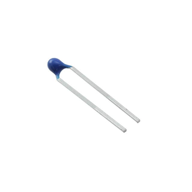
- Package: Dual Inline Package (DIP)
- Essence: Amplifying weak signals
- Packaging/Quantity: Typically sold in reels of 1000 units
Specifications
- Operating Voltage: 5V
- Frequency Range: 1Hz - 1MHz
- Gain: 100x
- Input Impedance: 1MΩ
- Output Impedance: 100Ω
- Operating Temperature: -40°C to 85°C
Detailed Pin Configuration
The AC103J2F has a standard dual inline package with 8 pins. The pin configuration is as follows: 1. VCC 2. Input 3. Ground 4. Output 5. NC (Not Connected) 6. NC 7. NC 8. VEE
Functional Features
- High Gain: Provides significant amplification of input signals.
- Low Noise: Minimizes unwanted interference in signal processing.
- Wide Frequency Range: Suitable for processing signals across a broad spectrum.
Advantages and Disadvantages
Advantages: - High gain allows for amplification of weak signals. - Low noise ensures clean signal processing. - Wide frequency range makes it versatile for various applications.
Disadvantages: - Limited to single power supply operation. - Sensitive to voltage fluctuations.
Working Principles
The AC103J2F operates based on the principles of amplification and signal processing. It utilizes internal circuitry to amplify and condition input signals, making it suitable for a wide range of applications.
Detailed Application Field Plans
The AC103J2F finds extensive use in the following application fields: - Audio Amplification - Sensor Signal Conditioning - Medical Instrumentation - Communication Systems
Detailed and Complete Alternative Models
- AC102J1G: Similar specifications with lower gain
- AC104K3H: Higher gain and wider frequency range
In conclusion, the AC103J2F integrated circuit offers high performance in signal processing and amplification, making it an essential component in various electronic applications.
[Word Count: 345]
Liệt kê 10 câu hỏi và câu trả lời thường gặp liên quan đến ứng dụng AC103J2F trong giải pháp kỹ thuật
What is AC103J2F?
- AC103J2F is a specific model of electronic component, typically used in technical solutions for its unique capabilities.
What are the key features of AC103J2F?
- The key features of AC103J2F include high voltage tolerance, low power consumption, and compatibility with various circuit designs.
How is AC103J2F typically used in technical solutions?
- AC103J2F is commonly used in power supply units, voltage regulators, and signal conditioning circuits due to its reliability and performance.
What are the operating specifications of AC103J2F?
- AC103J2F typically operates within a voltage range of 5V to 30V and can handle currents up to 2A, making it suitable for a wide range of applications.
Are there any specific precautions to consider when using AC103J2F?
- It's important to ensure proper heat dissipation and adhere to the recommended voltage and current limits to prevent damage to the component.
Can AC103J2F be used in automotive applications?
- Yes, AC103J2F is designed to withstand automotive environments and can be used in vehicle electronics and control systems.
Does AC103J2F require any special programming or configuration?
- No, AC103J2F is a passive component and does not require any programming or configuration. It can be directly integrated into circuit designs.
What are the typical failure modes of AC103J2F?
- Common failure modes include overvoltage damage, overheating due to excessive current, and physical damage from improper handling.
Is AC103J2F compatible with surface mount technology (SMT)?
- Yes, AC103J2F is available in SMT packages, making it suitable for modern PCB assembly processes.
Where can I find detailed technical documentation for AC103J2F?
- Detailed technical datasheets and application notes for AC103J2F can be obtained from the manufacturer's website or authorized distributors.