

Xem thông số kỹ thuật để biết chi tiết sản phẩm.
XA3S400A-4FGG400Q
Product Overview
Category: Integrated Circuit (IC)
Use: The XA3S400A-4FGG400Q is a programmable logic device used for digital circuit design and implementation. It offers high-performance and flexibility, making it suitable for various applications.
Characteristics: - Programmable logic device - High-performance - Flexible design options - Versatile application possibilities
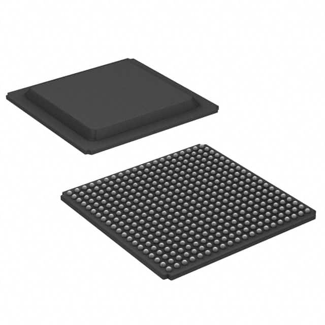
Package: The XA3S400A-4FGG400Q comes in a compact and durable package that ensures protection during handling and transportation. The package is designed to facilitate easy integration into electronic systems.
Essence: The XA3S400A-4FGG400Q is an essential component in digital circuit design, providing the ability to create custom logic functions and implement complex algorithms.
Packaging/Quantity: Each XA3S400A-4FGG400Q is individually packaged to ensure its integrity. The quantity per package may vary depending on the supplier or manufacturer.
Specifications
The XA3S400A-4FGG400Q has the following specifications:
- Logic Cells: 400
- Flip-Flops: 1,200
- Look-Up Tables (LUTs): 800
- Maximum Frequency: 400 MHz
- I/O Pins: 400
- Operating Voltage: 1.2V
- Package Type: FG(G)400
- Temperature Range: -40°C to +85°C
Detailed Pin Configuration
The XA3S400A-4FGG400Q has a specific pin configuration that enables connectivity with other components. The detailed pin configuration can be found in the product datasheet provided by the manufacturer.
Functional Features
The XA3S400A-4FGG400Q offers several functional features that enhance its usability and performance:
- Programmability: The device can be programmed to implement custom logic functions, allowing for flexibility in circuit design.
- High-Speed Operation: With a maximum frequency of 400 MHz, the XA3S400A-4FGG400Q can handle complex operations efficiently.
- Versatile I/O Options: The device provides 400 I/O pins, enabling seamless integration with other components and external devices.
- Low Power Consumption: The XA3S400A-4FGG400Q is designed to operate at low power, making it suitable for battery-powered applications.
Advantages and Disadvantages
Advantages: - Flexibility in circuit design - High-performance operation - Versatile I/O options - Low power consumption
Disadvantages: - Limited logic cells compared to higher-end models - Higher cost compared to simpler programmable logic devices
Working Principles
The XA3S400A-4FGG400Q operates based on the principles of programmable logic. It consists of configurable logic blocks (CLBs), interconnect resources, and I/O blocks. The CLBs contain look-up tables and flip-flops that can be programmed to implement desired logic functions. The interconnect resources provide connectivity between different CLBs and I/O blocks. By configuring the CLBs and interconnect resources, the XA3S400A-4FGG400Q can perform various digital logic operations.
Detailed Application Field Plans
The XA3S400A-4FGG400Q finds applications in various fields, including:
- Communications: Used in networking equipment, routers, and switches for data processing and protocol handling.
- Industrial Automation: Employed in control systems, PLCs, and robotics for real-time control and monitoring.
- Consumer Electronics: Integrated into smart devices, gaming consoles, and multimedia systems for enhanced functionality.
- Automotive: Utilized in automotive electronics for engine control, driver assistance systems, and infotainment.
Detailed and Complete Alternative Models
- XA3S200A-4FGG400Q: A lower-capacity version of the XA3S400A-4FGG400Q with 200 logic cells and 600 flip-flops.
- XA3S1000A-4FGG400Q: A higher-capacity model with 1000 logic cells and 3000 flip-flops, suitable for more complex designs.
- XA3S250E-4FGG400Q: An alternative model with a different architecture, offering 250 logic cells and additional features.
These alternative models provide options for different design requirements and project budgets.
In conclusion, the XA3S400A-4FGG400Q is a versatile programmable logic device that offers high-performance and flexibility in digital circuit design. Its functional features, advantages, and application field plans make it a valuable component in various industries.
Liệt kê 10 câu hỏi và câu trả lời thường gặp liên quan đến ứng dụng XA3S400A-4FGG400Q trong giải pháp kỹ thuật
Sure! Here are 10 common questions and answers related to the application of XA3S400A-4FGG400Q in technical solutions:
Question: What is the XA3S400A-4FGG400Q?
Answer: The XA3S400A-4FGG400Q is a specific model of field-programmable gate array (FPGA) manufactured by Xilinx.Question: What are the key features of the XA3S400A-4FGG400Q?
Answer: Some key features include 400,000 system gates, 400 MHz performance, 400 I/O pins, and a FGGB400 package.Question: What are the typical applications for the XA3S400A-4FGG400Q?
Answer: This FPGA can be used in various applications such as industrial automation, telecommunications, automotive electronics, and high-performance computing.Question: How can I program the XA3S400A-4FGG400Q?
Answer: You can program the FPGA using Xilinx's Vivado Design Suite or other compatible programming tools.Question: Can I reprogram the XA3S400A-4FGG400Q after it has been programmed once?
Answer: Yes, FPGAs are designed to be reprogrammable, allowing you to modify the functionality of the device as needed.Question: What is the power supply requirement for the XA3S400A-4FGG400Q?
Answer: The recommended power supply voltage for this FPGA is typically 1.2V, but it can operate within a range of 1.14V to 1.26V.Question: Does the XA3S400A-4FGG400Q support different communication protocols?
Answer: Yes, this FPGA supports various communication protocols such as UART, SPI, I2C, Ethernet, and PCIe.Question: Can I interface the XA3S400A-4FGG400Q with external memory devices?
Answer: Yes, this FPGA has dedicated memory interfaces that allow you to connect external memory devices like DDR3 or DDR4 SDRAM.Question: What is the maximum operating temperature for the XA3S400A-4FGG400Q?
Answer: The maximum junction temperature for this FPGA is typically 100°C, but it is recommended to refer to the datasheet for precise specifications.Question: Are there any development boards available for the XA3S400A-4FGG400Q?
Answer: Yes, Xilinx provides development boards like the Arty A7-35T or Basys 3, which are compatible with the XA3S400A-4FGG400Q FPGA.
Please note that the answers provided here are general and may vary depending on specific requirements and use cases. It is always recommended to refer to the official documentation and datasheets for accurate information.