

Xem thông số kỹ thuật để biết chi tiết sản phẩm.
XC2S150-5FGG456I
Product Overview
Category
XC2S150-5FGG456I belongs to the category of Field Programmable Gate Arrays (FPGAs).
Use
FPGAs are integrated circuits that can be programmed or reprogrammed after manufacturing. They are widely used in various electronic applications, including telecommunications, automotive, aerospace, and consumer electronics.
Characteristics
- High flexibility: FPGAs can be customized to perform specific functions by programming the logic gates and interconnections.
- Parallel processing: FPGAs can execute multiple tasks simultaneously, making them suitable for high-performance computing.
- Reconfigurability: FPGAs can be reprogrammed to adapt to changing requirements or to fix errors without replacing the hardware.
- Low power consumption: FPGAs offer efficient power management features, making them energy-efficient compared to other programmable devices.
Package and Quantity
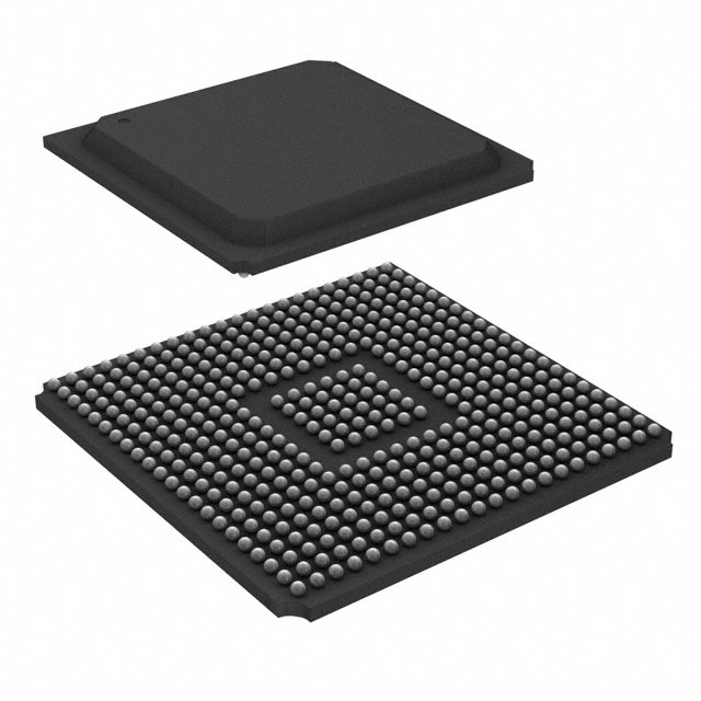
XC2S150-5FGG456I is available in a specific package type known as Fine-Pitch Ball Grid Array (FBGA). It comes in a quantity of one unit per package.
Specifications
- Model: XC2S150-5FGG456I
- Speed Grade: 5
- Logic Cells: 150,000
- I/O Pins: 456
- Operating Voltage: 3.3V
- Package Type: FBGA
- Temperature Range: -40°C to +100°C
Detailed Pin Configuration
The detailed pin configuration of XC2S150-5FGG456I can be found in the product datasheet provided by the manufacturer. It includes information about the function and connectivity of each pin on the FPGA.
Functional Features
XC2S150-5FGG456I offers the following functional features: - High-speed performance: The FPGA operates at a high clock frequency, enabling rapid data processing. - Programmable logic: The device allows users to implement complex digital logic functions using configurable logic blocks (CLBs). - Embedded memory: XC2S150-5FGG456I includes embedded memory blocks for storing data efficiently. - I/O flexibility: The FPGA provides a wide range of I/O pins, allowing easy interfacing with external devices. - Built-in DSP capabilities: The device incorporates digital signal processing (DSP) blocks, enabling efficient signal processing tasks.
Advantages and Disadvantages
Advantages
- Flexibility: FPGAs can be customized to meet specific application requirements, providing design flexibility.
- Reconfigurability: The ability to reprogram the FPGA allows for iterative development and quick prototyping.
- Parallel processing: FPGAs excel at parallel computing tasks, making them suitable for high-performance applications.
- Lower development costs: Using FPGAs can reduce the need for custom ASIC designs, resulting in cost savings.
Disadvantages
- Complexity: Designing for FPGAs requires specialized knowledge and expertise, which may increase development time and effort.
- Power consumption: FPGAs can consume more power compared to dedicated application-specific integrated circuits (ASICs).
- Higher cost: FPGAs are generally more expensive than off-the-shelf microcontrollers or processors.
Working Principles
FPGAs consist of an array of configurable logic blocks interconnected by programmable routing resources. The logic blocks contain look-up tables (LUTs), flip-flops, and other components that can be programmed to implement desired logic functions. The interconnections between these blocks can be configured to establish desired data paths. When programmed, the FPGA executes the desired logic operations based on the input signals received.
Detailed Application Field Plans
XC2S150-5FGG456I finds applications in various fields, including: 1. Telecommunications: Used in base stations, routers, and network switches for high-speed data processing and protocol handling. 2. Automotive: Employed in advanced driver-assistance systems (ADAS), engine control units (ECUs), and infotainment systems for real-time processing and control. 3. Aerospace: Utilized in satellite communication systems, avionics, and radar systems for signal processing and control functions. 4. Consumer Electronics: Found in smart TVs, gaming consoles, and digital cameras for image and video processing, as well as user interface control.
Detailed and Complete Alternative Models
- XC2S50-5FGG456I: A lower-capacity FPGA with 50,000 logic cells and 456 I/O pins.
- XC2S200-5FGG456I: A higher-capacity FPGA with 200,000 logic cells and 456 I/O pins.
- XC2S300-5FGG456I: An even higher-capacity FPGA with 300,000 logic cells and 456 I/O pins.
These alternative models provide different capacity options to suit various application requirements.
In conclusion, XC2S150-5FGG456I is a
Liệt kê 10 câu hỏi và câu trả lời thường gặp liên quan đến ứng dụng XC2S150-5FGG456I trong giải pháp kỹ thuật
Sure! Here are 10 common questions and answers related to the application of XC2S150-5FGG456I in technical solutions:
Question: What is XC2S150-5FGG456I?
Answer: XC2S150-5FGG456I is a specific model of Field Programmable Gate Array (FPGA) manufactured by Xilinx.Question: What are the key features of XC2S150-5FGG456I?
Answer: Some key features of XC2S150-5FGG456I include 150,000 system gates, 456-pin Fine-Pitch Ball Grid Array (FBGA) package, and a maximum operating frequency of 500 MHz.Question: What are the typical applications of XC2S150-5FGG456I?
Answer: XC2S150-5FGG456I is commonly used in various technical solutions such as digital signal processing, embedded systems, telecommunications, aerospace, and industrial automation.Question: How can XC2S150-5FGG456I be programmed?
Answer: XC2S150-5FGG456I can be programmed using Xilinx's Vivado Design Suite or ISE Design Suite software tools.Question: What is the power supply requirement for XC2S150-5FGG456I?
Answer: XC2S150-5FGG456I requires a single power supply voltage of 1.2V.Question: Can XC2S150-5FGG456I be used in high-speed applications?
Answer: Yes, XC2S150-5FGG456I has a maximum operating frequency of 500 MHz, making it suitable for high-speed applications.Question: Does XC2S150-5FGG456I support external memory interfaces?
Answer: Yes, XC2S150-5FGG456I supports various external memory interfaces such as DDR, DDR2, and DDR3.Question: Can XC2S150-5FGG456I be used in safety-critical applications?
Answer: Yes, XC2S150-5FGG456I can be used in safety-critical applications as long as it is properly designed and validated according to the required safety standards.Question: Are there any development boards available for XC2S150-5FGG456I?
Answer: Yes, Xilinx provides development boards like the Spartan-6 FPGA SP601 Evaluation Kit that can be used with XC2S150-5FGG456I.Question: What are the advantages of using XC2S150-5FGG456I in technical solutions?
Answer: Some advantages of using XC2S150-5FGG456I include its high gate count, flexibility, reprogrammability, and ability to handle complex digital designs efficiently.