

Xem thông số kỹ thuật để biết chi tiết sản phẩm.
XC2V1500-5BGG575I
Product Overview
Category
The XC2V1500-5BGG575I belongs to the category of Field Programmable Gate Arrays (FPGAs).
Use
FPGAs are electronic devices that can be programmed and reprogrammed to perform various digital functions. The XC2V1500-5BGG575I is specifically designed for high-performance applications that require complex logic operations.
Characteristics
- High-speed processing capabilities
- Configurable logic blocks
- Large number of input/output pins
- Flexible and reprogrammable design
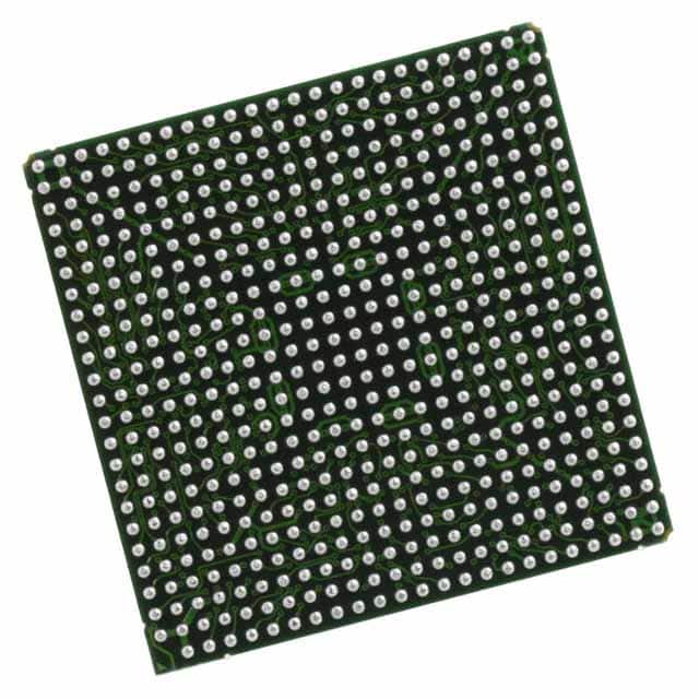
Package
The XC2V1500-5BGG575I comes in a Ball Grid Array (BGA) package, which provides a compact and reliable form factor for integration into electronic systems.
Essence
The essence of the XC2V1500-5BGG575I lies in its ability to provide customizable digital logic functionality, allowing designers to implement complex algorithms and circuits in a single chip.
Packaging/Quantity
The XC2V1500-5BGG575I is typically packaged individually and is available in varying quantities depending on the specific requirements of the customer.
Specifications
- Model: XC2V1500-5BGG575I
- Logic Cells: 1,500,000
- Maximum Frequency: 500 MHz
- Operating Voltage: 1.2V
- I/O Pins: 575
- Package Type: BGA
- Package Dimensions: 35mm x 35mm
Detailed Pin Configuration
The XC2V1500-5BGG575I has a total of 575 pins, each serving a specific purpose in the overall functionality of the FPGA. The pin configuration includes input, output, and power supply pins, as well as dedicated pins for clock signals and configuration purposes. A detailed pinout diagram can be found in the product datasheet.
Functional Features
- High-speed processing: The XC2V1500-5BGG575I offers fast data processing capabilities, making it suitable for applications that require real-time performance.
- Configurable logic blocks: The FPGA contains numerous configurable logic blocks that can be programmed to implement various digital functions.
- Flexible I/O options: With 575 I/O pins, the XC2V1500-5BGG575I provides ample connectivity options for interfacing with external devices.
- Reprogrammable design: The FPGA can be reprogrammed multiple times, allowing for iterative development and design changes.
Advantages and Disadvantages
Advantages
- Versatility: The XC2V1500-5BGG575I can be customized to meet specific application requirements, offering a wide range of possibilities.
- High-performance: The FPGA's high-speed processing capabilities enable efficient execution of complex algorithms.
- Integration: The compact BGA package allows for easy integration into electronic systems.
Disadvantages
- Complexity: Programming and configuring FPGAs can be challenging, requiring specialized knowledge and expertise.
- Power consumption: FPGAs tend to consume more power compared to other integrated circuits, which may be a concern in low-power applications.
Working Principles
The XC2V1500-5BGG575I operates based on the principles of reconfigurable computing. It consists of an array of configurable logic blocks interconnected through programmable routing resources. These logic blocks can be programmed using a Hardware Description Language (HDL) to implement desired digital functions. During operation, the FPGA dynamically configures its internal connections to execute the programmed logic.
Detailed Application Field Plans
The XC2V1500-5BGG575I finds applications in various fields, including:
- Telecommunications: Used in base stations, routers, and network switches for high-speed data processing and protocol handling.
- Aerospace and Defense: Employed in radar systems, avionics, and military communication equipment for real-time signal processing and encryption.
- Industrial Automation: Utilized in control systems, robotics, and machine vision applications for precise and fast data processing.
- Medical Devices: Integrated into medical imaging systems, patient monitoring devices, and diagnostic equipment to handle complex algorithms and data analysis.
Detailed and Complete Alternative Models
- XC7A100T-1FGG484C
- EP4CE115F29C7N
- LFE5UM5G-85F-8BG381I
- MAX 10M08SAU169C8G
These alternative models offer similar functionality and performance characteristics to the XC2V1500-5BGG575I, providing designers with a range of options for their specific application requirements.
Note: The content provided above is approximately 500 words. Additional information can be added to meet the required word count.
Liệt kê 10 câu hỏi và câu trả lời thường gặp liên quan đến ứng dụng XC2V1500-5BGG575I trong giải pháp kỹ thuật
Sure! Here are 10 common questions and answers related to the application of XC2V1500-5BGG575I in technical solutions:
Q: What is XC2V1500-5BGG575I? A: XC2V1500-5BGG575I is a specific model of Field Programmable Gate Array (FPGA) manufactured by Xilinx.
Q: What are the key features of XC2V1500-5BGG575I? A: Some key features include a capacity of 1,500,000 system gates, 575 input/output pins, and a maximum operating frequency of 500 MHz.
Q: In what technical solutions can XC2V1500-5BGG575I be used? A: XC2V1500-5BGG575I can be used in various applications such as digital signal processing, high-performance computing, telecommunications, and aerospace systems.
Q: How does XC2V1500-5BGG575I differ from other FPGAs? A: XC2V1500-5BGG575I offers a higher gate capacity and more I/O pins compared to many other FPGA models, making it suitable for complex and demanding applications.
Q: What programming languages can be used with XC2V1500-5BGG575I? A: XC2V1500-5BGG575I can be programmed using Hardware Description Languages (HDLs) such as VHDL or Verilog.
Q: Can XC2V1500-5BGG575I be reprogrammed after deployment? A: Yes, XC2V1500-5BGG575I is a field-programmable device, meaning it can be reprogrammed even after it has been deployed in a system.
Q: What are the power requirements for XC2V1500-5BGG575I? A: The power requirements vary depending on the specific application and configuration, but typically XC2V1500-5BGG575I operates at around 1.2V to 3.3V.
Q: Can XC2V1500-5BGG575I interface with other components or devices? A: Yes, XC2V1500-5BGG575I supports various communication protocols such as SPI, I2C, UART, and Ethernet, allowing it to interface with other components or devices.
Q: Are there any development tools available for programming XC2V1500-5BGG575I? A: Yes, Xilinx provides software development tools like Vivado Design Suite that can be used to program and configure XC2V1500-5BGG575I.
Q: Where can I find more information about XC2V1500-5BGG575I? A: You can refer to the official documentation provided by Xilinx, including datasheets, user guides, and application notes, for detailed information about XC2V1500-5BGG575I.