

Xem thông số kỹ thuật để biết chi tiết sản phẩm.
XC2V500-4FGG456C
Product Overview
Category
XC2V500-4FGG456C belongs to the category of Field Programmable Gate Arrays (FPGAs).
Use
This product is primarily used in digital logic circuits for various applications such as telecommunications, automotive, aerospace, and consumer electronics.
Characteristics
- High-performance programmable logic device
- Offers flexibility and reconfigurability
- Provides high-speed data processing capabilities
- Supports complex algorithms and designs
- Low power consumption
- Scalable architecture
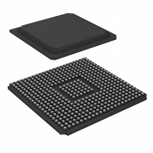
Package
XC2V500-4FGG456C is available in a compact and durable package that ensures protection during handling and transportation. The package is designed to withstand harsh environmental conditions.
Essence
The essence of XC2V500-4FGG456C lies in its ability to provide a customizable and versatile solution for implementing complex digital systems. It allows designers to create and modify logic circuits according to their specific requirements.
Packaging/Quantity
XC2V500-4FGG456C is typically packaged individually and is available in varying quantities depending on the customer's needs.
Specifications
- FPGA Family: Virtex-II
- Logic Cells: 5,136
- Number of I/Os: 456
- Operating Voltage: 3.3V
- Maximum Frequency: 200 MHz
- Embedded Block RAM: 576 Kb
- Total Distributed RAM: 1,152 Kb
- Configuration Memory: 4 Mb PROM
Detailed Pin Configuration
The XC2V500-4FGG456C has a total of 456 pins, each serving a specific purpose in the circuit design. The pin configuration includes input/output pins, clock pins, power supply pins, and configuration pins. For a detailed pin configuration diagram, please refer to the datasheet provided by the manufacturer.
Functional Features
- High-speed data processing capabilities
- Configurable logic blocks for implementing complex algorithms
- Flexible I/O options for interfacing with external devices
- On-chip memory resources for efficient data storage and retrieval
- Built-in configuration memory for easy reprogramming
- Support for various communication protocols
Advantages and Disadvantages
Advantages
- Flexibility and reconfigurability allow for rapid prototyping and design iterations.
- High-performance capabilities enable the implementation of complex algorithms and designs.
- Low power consumption makes it suitable for battery-powered applications.
- Scalable architecture allows for future expansion and upgrades.
Disadvantages
- Initial setup and configuration can be time-consuming.
- Limited availability of alternative models may restrict design choices.
- Higher cost compared to fixed-function integrated circuits.
Working Principles
XC2V500-4FGG456C operates based on the principles of digital logic circuits. It consists of configurable logic blocks, interconnects, and input/output elements. The device can be programmed to implement specific logic functions by configuring the interconnections between logic blocks. The configuration is stored in the on-chip memory, allowing for reprogramming as needed.
Detailed Application Field Plans
XC2V500-4FGG456C finds applications in various fields, including:
- Telecommunications: Used in network routers, switches, and base stations for high-speed data processing and protocol handling.
- Automotive: Employed in advanced driver assistance systems (ADAS) for real-time image processing and sensor fusion.
- Aerospace: Utilized in avionics systems for flight control, navigation, and communication.
- Consumer Electronics: Integrated into smart TVs, gaming consoles, and multimedia devices for enhanced performance and functionality.
Detailed and Complete Alternative Models
While XC2V500-4FGG456C offers a range of features and capabilities, there are alternative models available in the market that cater to different requirements. Some notable alternatives include:
- XC2V1000-4FGG456C: Offers higher logic capacity and additional features for more demanding applications.
- XC2S50-5TQ144C: Provides a lower-cost option with reduced logic capacity suitable for simpler designs.
- XC7A35T-1CPG236C: Belongs to the newer generation of FPGAs, offering improved performance and power efficiency.
These alternative models can be considered based on specific project requirements and budget constraints.
In conclusion, XC2V500-4FGG456C is a high-performance FPGA that provides flexibility, reconfigurability, and scalability for implementing complex digital logic circuits. Its wide range of applications and compatibility with alternative models make it a versatile choice for various industries.
Liệt kê 10 câu hỏi và câu trả lời thường gặp liên quan đến ứng dụng XC2V500-4FGG456C trong giải pháp kỹ thuật
Sure! Here are 10 common questions and answers related to the application of XC2V500-4FGG456C in technical solutions:
Q: What is XC2V500-4FGG456C? A: XC2V500-4FGG456C is a field-programmable gate array (FPGA) manufactured by Xilinx. It offers 500,000 system gates and is designed for high-performance applications.
Q: What are some typical applications of XC2V500-4FGG456C? A: XC2V500-4FGG456C can be used in various technical solutions such as digital signal processing, telecommunications, aerospace, industrial automation, and scientific research.
Q: How does XC2V500-4FGG456C differ from other FPGAs? A: XC2V500-4FGG456C stands out due to its large number of system gates, which allows for complex designs and high-performance applications. It also offers advanced features like embedded memory blocks and built-in multipliers.
Q: Can XC2V500-4FGG456C be reprogrammed after deployment? A: Yes, XC2V500-4FGG456C is a field-programmable device, meaning it can be reprogrammed even after it has been deployed in a system.
Q: What development tools are available for programming XC2V500-4FGG456C? A: Xilinx provides software tools like Vivado Design Suite and ISE Design Suite that enable developers to program and configure XC2V500-4FGG456C.
Q: Is XC2V500-4FGG456C suitable for low-power applications? A: XC2V500-4FGG456C is not specifically optimized for low-power applications. However, power consumption can be managed by carefully designing the FPGA logic and utilizing power-saving techniques.
Q: Can XC2V500-4FGG456C interface with other components or devices? A: Yes, XC2V500-4FGG456C supports various standard interfaces like UART, SPI, I2C, and GPIOs, allowing it to communicate with other components or devices in a system.
Q: What are the temperature and voltage operating ranges of XC2V500-4FGG456C? A: XC2V500-4FGG456C typically operates within a temperature range of -40°C to 100°C and requires a supply voltage of 1.5V to 3.3V.
Q: Are there any limitations or considerations when using XC2V500-4FGG456C? A: Some considerations include the need for proper cooling due to high power consumption, careful planning of I/O requirements, and understanding the timing constraints of the design.
Q: Where can I find more information about XC2V500-4FGG456C and its application in technical solutions? A: You can refer to Xilinx's official website, product documentation, application notes, and online forums for more detailed information and resources related to XC2V500-4FGG456C.