

Xem thông số kỹ thuật để biết chi tiết sản phẩm.
XC2VP40-5FF1148C
Product Overview
Category
XC2VP40-5FF1148C belongs to the category of Field Programmable Gate Arrays (FPGAs).
Use
This product is primarily used in digital logic circuits for various applications such as telecommunications, automotive, aerospace, and consumer electronics.
Characteristics
- High-performance FPGA with advanced features
- Flexible and reconfigurable design
- Low power consumption
- High-speed data processing capabilities
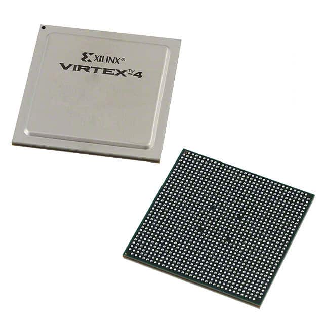
Package
XC2VP40-5FF1148C is available in a compact and durable package, ensuring easy integration into electronic systems.
Essence
The essence of XC2VP40-5FF1148C lies in its ability to provide a customizable hardware solution for complex digital designs.
Packaging/Quantity
XC2VP40-5FF1148C is typically packaged individually and is available in various quantities depending on customer requirements.
Specifications
- FPGA Family: Virtex-II Pro
- Logic Cells: 40,000
- System Gates: 1,152,000
- Block RAM: 864 Kb
- Maximum Frequency: 500 MHz
- I/O Pins: 1148
- Operating Voltage: 1.5V
- Package Type: FF1148
Detailed Pin Configuration
The detailed pin configuration of XC2VP40-5FF1148C can be found in the product datasheet provided by the manufacturer. It includes information about input/output pins, power supply pins, clock pins, and other necessary connections.
Functional Features
XC2VP40-5FF1148C offers several functional features that make it a versatile FPGA for various applications:
- Configurable logic blocks for implementing custom digital circuits
- Dedicated DSP slices for efficient signal processing
- Built-in memory blocks for data storage
- High-speed serial transceivers for fast data communication
- Flexible clock management resources for precise timing control
Advantages and Disadvantages
Advantages
- High-performance FPGA with advanced features
- Reconfigurable design allows for flexibility in system development
- Low power consumption compared to alternative solutions
- Excellent data processing capabilities for demanding applications
Disadvantages
- Relatively high cost compared to other programmable logic devices
- Steeper learning curve for inexperienced users
- Limited availability of technical support for complex designs
Working Principles
XC2VP40-5FF1148C operates based on the principles of reconfigurable hardware. It consists of a matrix of configurable logic blocks interconnected through programmable routing resources. The user can program the FPGA to implement desired digital circuits by configuring the interconnections and functionality of these logic blocks.
Detailed Application Field Plans
XC2VP40-5FF1148C finds applications in various fields, including:
- Telecommunications: Used in network routers, switches, and base stations for high-speed data processing.
- Automotive: Employed in automotive electronics for functions like engine control, driver assistance systems, and infotainment.
- Aerospace: Utilized in satellite communication systems, onboard computers, and avionics for reliable and efficient data processing.
- Consumer Electronics: Integrated into multimedia devices, gaming consoles, and smart home appliances for enhanced performance and functionality.
Detailed and Complete Alternative Models
Some alternative models to XC2VP40-5FF1148C that offer similar functionalities include:
- Xilinx Virtex-7 XC7VX485T-2FFG1761C
- Altera Stratix V 5SGXEA7N2F45C2LN
- Lattice ECP5-85F-6BG256C
These alternatives provide comparable performance and features, catering to different project requirements.
In conclusion, XC2VP40-5FF1148C is a high-performance FPGA belonging to the Virtex-II Pro family. With its advanced features, flexibility, and low power consumption, it serves as a versatile solution for various digital logic circuit applications in different industries.
Liệt kê 10 câu hỏi và câu trả lời thường gặp liên quan đến ứng dụng XC2VP40-5FF1148C trong giải pháp kỹ thuật
Sure! Here are 10 common questions and answers related to the application of XC2VP40-5FF1148C in technical solutions:
Q: What is XC2VP40-5FF1148C? A: XC2VP40-5FF1148C is a field-programmable gate array (FPGA) manufactured by Xilinx.
Q: What are the key features of XC2VP40-5FF1148C? A: Some key features include 40,000 logic cells, 1.2V core voltage, 5-speed grade, and 1148-pin BGA package.
Q: What applications can XC2VP40-5FF1148C be used for? A: XC2VP40-5FF1148C can be used in various applications such as telecommunications, networking, industrial automation, and high-performance computing.
Q: How does XC2VP40-5FF1148C differ from other FPGAs? A: XC2VP40-5FF1148C offers a balance between logic capacity, performance, and power consumption, making it suitable for a wide range of applications.
Q: What tools are available for programming XC2VP40-5FF1148C? A: Xilinx provides software tools like Vivado Design Suite that allow users to program and configure XC2VP40-5FF1148C.
Q: Can XC2VP40-5FF1148C be reprogrammed after deployment? A: Yes, XC2VP40-5FF1148C is a reprogrammable FPGA, allowing for flexibility and updates in the field.
Q: What are the power requirements for XC2VP40-5FF1148C? A: XC2VP40-5FF1148C requires a 1.2V core voltage and typically operates at low power consumption levels.
Q: Are there any development boards available for XC2VP40-5FF1148C? A: Yes, Xilinx offers development boards like the Virtex-II Pro Development System that are compatible with XC2VP40-5FF1148C.
Q: Can XC2VP40-5FF1148C interface with other components or devices? A: Yes, XC2VP40-5FF1148C supports various interfaces such as PCIe, Ethernet, USB, and DDR memory, allowing for seamless integration with other components.
Q: Where can I find more information about XC2VP40-5FF1148C? A: You can refer to the official Xilinx website, datasheets, application notes, or reach out to Xilinx support for detailed information on XC2VP40-5FF1148C.