

Xem thông số kỹ thuật để biết chi tiết sản phẩm.
XC2VP40-5FFG1148I
Basic Information Overview
- Category: Integrated Circuit (IC)
- Use: Programmable Logic Device (PLD)
- Characteristics: High-performance, high-density, field-programmable gate array (FPGA)
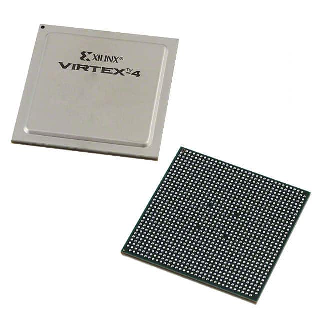
- Package: 1148-ball Flip Chip FineLine BGA (FFBGA)
- Essence: The XC2VP40-5FFG1148I is a versatile FPGA designed for various applications that require high-speed processing and programmability.
- Packaging/Quantity: Available in individual units or reels, depending on the manufacturer's packaging specifications.
Specifications
- Logic Cells: 40,000
- System Gates: 1.5 million
- Block RAM: 864 Kb
- DSP Slices: 192
- I/O Pins: 800
- Operating Voltage: 1.2V
- Maximum Frequency: 500 MHz
- Configuration Memory: Embedded Flash
Detailed Pin Configuration
The XC2VP40-5FFG1148I has a total of 1148 pins, each serving a specific purpose. The pin configuration includes power supply pins, ground pins, input/output pins, configuration pins, clock pins, and specialized pins for specific functionalities. A detailed pinout diagram can be found in the datasheet provided by the manufacturer.
Functional Features
- High-performance FPGA with advanced architecture for efficient processing.
- Flexible and reprogrammable logic cells allow for customization and adaptation to different applications.
- Large number of I/O pins enable connectivity with external devices and systems.
- Embedded memory blocks provide efficient storage and retrieval of data.
- Dedicated DSP slices enhance signal processing capabilities.
- Support for various communication protocols and interfaces.
Advantages and Disadvantages
Advantages: - Versatile and adaptable to a wide range of applications. - High-performance processing capabilities. - Large number of I/O pins for extensive connectivity options. - Efficient use of resources with embedded memory blocks and DSP slices.
Disadvantages: - Higher power consumption compared to other programmable logic devices. - Complex programming and configuration process may require expertise. - Limited availability of alternative models with similar specifications.
Working Principles
The XC2VP40-5FFG1148I operates based on the principles of field-programmable gate arrays (FPGAs). It consists of a matrix of configurable logic cells interconnected through programmable routing resources. The device can be programmed using hardware description languages (HDL) or specialized software tools, allowing users to define the desired functionality and interconnections within the FPGA. Once programmed, the XC2VP40-5FFG1148I executes the defined logic operations and data processing tasks.
Detailed Application Field Plans
The XC2VP40-5FFG1148I finds applications in various fields that require high-performance programmable logic devices. Some potential application areas include: - Telecommunications: FPGA-based signal processing, network protocol implementation. - Aerospace and Defense: Radar systems, avionics, secure communication systems. - Industrial Automation: Control systems, robotics, machine vision. - High-Performance Computing: Data centers, scientific simulations, cryptography. - Automotive: Advanced driver-assistance systems (ADAS), infotainment systems.
Detailed and Complete Alternative Models
While the XC2VP40-5FFG1148I offers unique features and specifications, there are alternative models available from different manufacturers that cater to similar requirements. Some notable alternatives include: - Xilinx Virtex-4 series FPGAs - Altera Stratix II series FPGAs - LatticeECP3 series FPGAs
These alternative models provide varying performance levels, resource capacities, and packaging options, allowing users to choose the most suitable FPGA for their specific application needs.
Note: The content provided above is a sample structure for an encyclopedia entry and may not reflect the actual specifications or details of the XC2VP40-5FFG1148I FPGA.
Liệt kê 10 câu hỏi và câu trả lời thường gặp liên quan đến ứng dụng XC2VP40-5FFG1148I trong giải pháp kỹ thuật
Sure! Here are 10 common questions and answers related to the application of XC2VP40-5FFG1148I in technical solutions:
Q: What is XC2VP40-5FFG1148I? A: XC2VP40-5FFG1148I is a specific model of Field Programmable Gate Array (FPGA) manufactured by Xilinx.
Q: What are the key features of XC2VP40-5FFG1148I? A: Some key features of XC2VP40-5FFG1148I include 40,000 logic cells, high-speed serial transceivers, embedded PowerPC processors, and support for various I/O standards.
Q: What are the typical applications of XC2VP40-5FFG1148I? A: XC2VP40-5FFG1148I is commonly used in applications such as telecommunications, networking, video processing, industrial automation, and high-performance computing.
Q: How can XC2VP40-5FFG1148I be programmed? A: XC2VP40-5FFG1148I can be programmed using Xilinx's Vivado Design Suite or ISE Design Suite software tools.
Q: What is the power consumption of XC2VP40-5FFG1148I? A: The power consumption of XC2VP40-5FFG1148I depends on the specific design and configuration, but it typically ranges from a few watts to tens of watts.
Q: Can XC2VP40-5FFG1148I be used in safety-critical applications? A: Yes, XC2VP40-5FFG1148I can be used in safety-critical applications, provided that the design and implementation meet the necessary safety standards and requirements.
Q: Does XC2VP40-5FFG1148I support high-speed serial communication? A: Yes, XC2VP40-5FFG1148I supports high-speed serial communication through its built-in transceivers, which can operate at multi-gigabit speeds.
Q: Can XC2VP40-5FFG1148I interface with other components or devices? A: Yes, XC2VP40-5FFG1148I can interface with various components and devices using different I/O standards such as LVCMOS, LVDS, and differential signaling.
Q: What is the maximum clock frequency supported by XC2VP40-5FFG1148I? A: The maximum clock frequency supported by XC2VP40-5FFG1148I depends on the specific design and implementation, but it can typically reach several hundred megahertz.
Q: Are there any known limitations or considerations when using XC2VP40-5FFG1148I? A: Some considerations include power supply requirements, thermal management, signal integrity, and proper design techniques to optimize performance and reliability.
Please note that these answers are general and may vary depending on specific design requirements and implementation details.