

Xem thông số kỹ thuật để biết chi tiết sản phẩm.
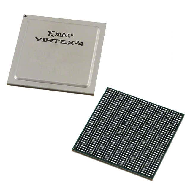
XC2VP40-6FFG1148C
Product Overview
Category
XC2VP40-6FFG1148C belongs to the category of Field Programmable Gate Arrays (FPGAs).
Use
This FPGA is primarily used for digital logic implementation and customization in various electronic systems.
Characteristics
- High-performance programmable logic device
- Offers flexibility and reconfigurability
- Provides high-speed data processing capabilities
- Supports complex digital designs
- Enables rapid prototyping and development
Package
XC2VP40-6FFG1148C comes in a Flip-Chip Fine-Pitch Ball Grid Array (FFGBA) package.
Essence
The essence of XC2VP40-6FFG1148C lies in its ability to provide a versatile platform for implementing custom digital circuits with high performance and flexibility.
Packaging/Quantity
XC2VP40-6FFG1148C is typically packaged individually and is available in various quantities depending on customer requirements.
Specifications
- FPGA Family: Virtex-II Pro
- Logic Cells: 40,000
- System Gates: 1,000,000
- Maximum Frequency: 500 MHz
- I/O Pins: 1148
- Operating Voltage: 3.3V
- Package Type: FFGBA
- Temperature Range: -40°C to +100°C
Detailed Pin Configuration
The pin configuration of XC2VP40-6FFG1148C is as follows:
- Pin 1: VCCINT
- Pin 2: GND
- Pin 3: VCCINT
- ...
- Pin 1148: IOB_1139
For a complete pin configuration diagram, please refer to the datasheet provided by the manufacturer.
Functional Features
XC2VP40-6FFG1148C offers the following functional features:
- Programmable logic cells for implementing custom digital circuits
- Embedded PowerPC processor cores for system integration
- High-speed serial transceivers for data communication
- Memory interfaces for efficient data storage and retrieval
- Clock management resources for precise timing control
Advantages and Disadvantages
Advantages
- Flexibility to implement custom digital designs
- Reconfigurability for rapid prototyping and development
- High-performance capabilities for demanding applications
- Integration of processor cores for system-level functionality
Disadvantages
- Higher cost compared to fixed-function integrated circuits
- Steeper learning curve for programming and design implementation
- Limited availability of alternative models with similar specifications
Working Principles
XC2VP40-6FFG1148C operates based on the principles of reconfigurable logic. It consists of a matrix of programmable logic cells interconnected through configurable routing resources. These logic cells can be programmed to implement various digital functions, allowing users to create custom circuits tailored to their specific requirements. The configuration of the FPGA is stored in internal memory elements, which can be modified to change the behavior of the device.
Detailed Application Field Plans
XC2VP40-6FFG1148C finds applications in a wide range of fields, including:
- Telecommunications: Used in base stations, network switches, and routers for high-speed data processing.
- Aerospace and Defense: Employed in radar systems, avionics, and military communication equipment for reliable and customizable digital signal processing.
- Industrial Automation: Integrated into control systems, robotics, and machine vision applications for real-time data processing and control.
- Medical Devices: Utilized in medical imaging, patient monitoring, and diagnostic equipment for high-performance data processing and analysis.
- Automotive: Incorporated into advanced driver assistance systems (ADAS), infotainment systems, and engine control units (ECUs) for enhanced functionality and performance.
Detailed and Complete Alternative Models
While XC2VP40-6FFG1148C is a highly capable FPGA, there are alternative models available with similar specifications. Some notable alternatives include:
- Xilinx Virtex-7 XC7VX485T: Offers higher logic capacity and improved performance.
- Intel Stratix 10 GX: Provides advanced features like high-speed transceivers and embedded processors.
- Lattice ECP5: Offers a cost-effective solution with lower power consumption.
These alternative models can be considered based on specific project requirements and budget constraints.
In conclusion, XC2VP40-6FFG1148C is a versatile FPGA that enables the implementation of custom digital circuits with high performance and flexibility. Its wide range of applications, functional features, and availability of alternative models make it a valuable choice for various electronic systems.
Liệt kê 10 câu hỏi và câu trả lời thường gặp liên quan đến ứng dụng XC2VP40-6FFG1148C trong giải pháp kỹ thuật
Sure! Here are 10 common questions and answers related to the application of XC2VP40-6FFG1148C in technical solutions:
1. What is XC2VP40-6FFG1148C? - XC2VP40-6FFG1148C is a specific model of Field Programmable Gate Array (FPGA) manufactured by Xilinx.
2. What are the key features of XC2VP40-6FFG1148C? - XC2VP40-6FFG1148C offers 40,000 logic cells, 1,152 Kb of block RAM, 640 DSP slices, and supports various I/O standards.
3. In what applications can XC2VP40-6FFG1148C be used? - XC2VP40-6FFG1148C can be used in a wide range of applications such as telecommunications, networking, industrial automation, image processing, and more.
4. What is the maximum operating frequency of XC2VP40-6FFG1148C? - The maximum operating frequency of XC2VP40-6FFG1148C depends on the design and implementation, but it can typically reach frequencies up to several hundred megahertz.
5. How can I program XC2VP40-6FFG1148C? - XC2VP40-6FFG1148C can be programmed using Xilinx's Vivado Design Suite or ISE Design Suite software tools.
6. Can XC2VP40-6FFG1148C be reprogrammed after deployment? - Yes, XC2VP40-6FFG1148C is a reprogrammable FPGA, allowing for updates and modifications to the design even after deployment.
7. What are the power requirements for XC2VP40-6FFG1148C? - The power requirements for XC2VP40-6FFG1148C vary depending on the specific design and usage, but typically it operates at a voltage of 1.2V.
8. Does XC2VP40-6FFG1148C support high-speed serial interfaces? - Yes, XC2VP40-6FFG1148C supports various high-speed serial interfaces such as PCIe, SATA, Ethernet, and more.
9. Can XC2VP40-6FFG1148C interface with external memory devices? - Yes, XC2VP40-6FFG1148C has built-in block RAM and can also interface with external memory devices like DDR SDRAM or Flash memory.
10. Are there any development boards available for XC2VP40-6FFG1148C? - Yes, Xilinx provides development boards like the Virtex-II Pro Development System that are specifically designed for prototyping and testing with XC2VP40-6FFG1148C.
Please note that the answers provided here are general and may vary based on specific implementation details and requirements.