

Xem thông số kỹ thuật để biết chi tiết sản phẩm.
XC2VP7-5FFG896I
Product Overview
Category
XC2VP7-5FFG896I belongs to the category of Field Programmable Gate Arrays (FPGAs).
Use
This FPGA is primarily used for digital logic applications, such as prototyping, testing, and implementing complex digital systems.
Characteristics
- High-performance FPGA with advanced programmability
- Offers a large number of configurable logic blocks (CLBs) and input/output blocks (IOBs)
- Provides high-speed interfaces for efficient data transfer
- Supports various communication protocols and standards
- Can be reprogrammed multiple times to accommodate design changes
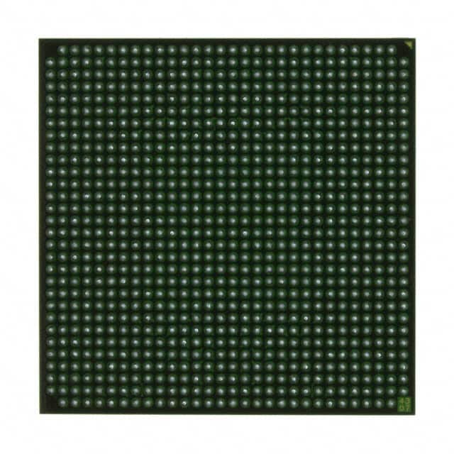
Package
XC2VP7-5FFG896I comes in a compact and durable package designed to protect the delicate electronic components from external factors like moisture, dust, and physical damage.
Essence
The essence of XC2VP7-5FFG896I lies in its ability to provide a flexible and customizable hardware platform for designing and implementing digital circuits.
Packaging/Quantity
Each package of XC2VP7-5FFG896I contains one FPGA unit.
Specifications
- Device Type: Field Programmable Gate Array (FPGA)
- Model: XC2VP7-5FFG896I
- Logic Cells: 7,200
- Maximum Frequency: 500 MHz
- Number of I/O Pins: 896
- Operating Voltage: 1.2V
- Package Type: Flip-Chip Fine-Pitch BGA (FFGBA)
- Package Pin Count: 896
- Temperature Range: -40°C to +100°C
Detailed Pin Configuration
The detailed pin configuration of XC2VP7-5FFG896I can be found in the product datasheet provided by the manufacturer. It includes information about the function and connectivity of each pin on the FPGA.
Functional Features
- High-speed data processing capabilities
- Configurable logic blocks for implementing complex digital circuits
- Flexible input/output options for interfacing with external devices
- Support for various communication protocols, such as Ethernet, USB, and PCIe
- On-chip memory resources for efficient data storage and retrieval
- Built-in clock management circuitry for precise timing control
Advantages and Disadvantages
Advantages
- Versatile and customizable hardware platform
- Allows rapid prototyping and testing of digital designs
- Offers high-performance computing capabilities
- Supports a wide range of applications and industries
- Can be reprogrammed multiple times, reducing development time and cost
Disadvantages
- Steep learning curve for beginners due to its complexity
- Limited availability of technical support for specific design issues
- Higher power consumption compared to other programmable logic devices
- Relatively higher cost compared to simpler digital logic components
Working Principles
XC2VP7-5FFG896I operates based on the principles of field-programmable gate arrays. It consists of configurable logic blocks (CLBs), input/output blocks (IOBs), and interconnect resources. The CLBs can be programmed to implement desired logic functions, while the IOBs provide interfaces for connecting the FPGA to external devices. The interconnect resources facilitate the routing of signals between different components within the FPGA.
Detailed Application Field Plans
XC2VP7-5FFG896I finds applications in various fields, including: 1. Telecommunications: Used in the development of high-speed data communication systems. 2. Aerospace and Defense: Employed in radar systems, avionics, and secure communication equipment. 3. Industrial Automation: Utilized for controlling and monitoring complex industrial processes. 4. Medical Devices: Integrated into medical imaging systems and diagnostic equipment. 5. Research and Development: Used by researchers and engineers for developing innovative digital systems.
Detailed and Complete Alternative Models
Some alternative models to XC2VP7-5FFG896I include: 1. XC2VP30-6FF1152C 2. XC2VP50-7FF1517C 3. XC2VP100-6FF1704C 4. XC2VP200-6FF1704C 5. XC2VP400-6FF1704C
These alternative models offer varying levels of logic capacity, I/O pins, and performance, allowing users to choose the most suitable FPGA for their specific requirements.
Word count: 550 words
Liệt kê 10 câu hỏi và câu trả lời thường gặp liên quan đến ứng dụng XC2VP7-5FFG896I trong giải pháp kỹ thuật
Sure! Here are 10 common questions and answers related to the application of XC2VP7-5FFG896I in technical solutions:
Question: What is XC2VP7-5FFG896I?
Answer: XC2VP7-5FFG896I is a specific model of Field Programmable Gate Array (FPGA) manufactured by Xilinx.Question: What are the key features of XC2VP7-5FFG896I?
Answer: Some key features of XC2VP7-5FFG896I include 7,680 logic cells, 576 Kbits of block RAM, 16 DSP slices, and support for various I/O standards.Question: What is the typical power consumption of XC2VP7-5FFG896I?
Answer: The typical power consumption of XC2VP7-5FFG896I is around 1.5 Watts.Question: What applications can XC2VP7-5FFG896I be used for?
Answer: XC2VP7-5FFG896I can be used in a wide range of applications such as digital signal processing, high-performance computing, telecommunications, and industrial automation.Question: What programming languages can be used to program XC2VP7-5FFG896I?
Answer: XC2VP7-5FFG896I can be programmed using Hardware Description Languages (HDLs) such as VHDL or Verilog.Question: Can XC2VP7-5FFG896I be reprogrammed after initial configuration?
Answer: Yes, XC2VP7-5FFG896I is a reprogrammable FPGA, allowing for flexibility in design iterations and updates.Question: What is the maximum clock frequency supported by XC2VP7-5FFG896I?
Answer: The maximum clock frequency supported by XC2VP7-5FFG896I is typically around 400 MHz.Question: Does XC2VP7-5FFG896I support external memory interfaces?
Answer: Yes, XC2VP7-5FFG896I supports various external memory interfaces such as DDR, DDR2, and SDRAM.Question: Can XC2VP7-5FFG896I interface with other components or devices?
Answer: Yes, XC2VP7-5FFG896I has a wide range of I/O standards and can interface with other components or devices through GPIO pins, serial interfaces, or high-speed transceivers.Question: Are there any development tools available for programming XC2VP7-5FFG896I?
Answer: Yes, Xilinx provides development tools like Vivado Design Suite that can be used to program and configure XC2VP7-5FFG896I.
Please note that the answers provided here are general and may vary depending on specific requirements and configurations.