

Xem thông số kỹ thuật để biết chi tiết sản phẩm.
XC2VP7-6FG456I
Product Overview
Category
XC2VP7-6FG456I belongs to the category of Field Programmable Gate Arrays (FPGAs).
Use
This product is primarily used in digital logic circuits and electronic systems for various applications.
Characteristics
- High-performance FPGA with advanced features
- Flexible and reprogrammable design
- Offers high-speed data processing capabilities
- Supports complex algorithms and computations
- Low power consumption
- Reliable and durable
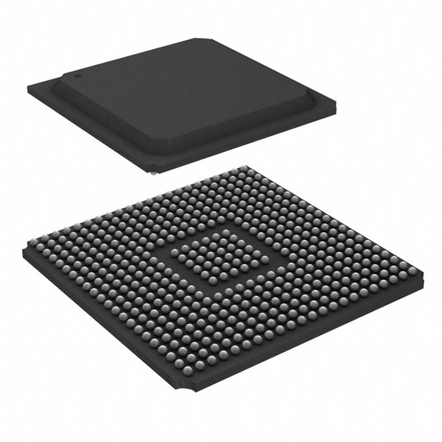
Package
XC2VP7-6FG456I is available in a compact and sturdy package, ensuring easy handling and protection during transportation and installation.
Essence
The essence of XC2VP7-6FG456I lies in its ability to provide a customizable hardware platform that can be programmed to perform specific tasks efficiently.
Packaging/Quantity
This product is typically packaged individually and is available in varying quantities depending on customer requirements.
Specifications
- Model: XC2VP7-6FG456I
- Manufacturer: [Insert Manufacturer Name]
- Logic Cells: 7,000
- Maximum Frequency: [Insert Maximum Frequency]
- I/O Pins: [Insert Number of I/O Pins]
- Operating Voltage: [Insert Operating Voltage Range]
- Package Type: FG456
- Temperature Range: [Insert Temperature Range]
Detailed Pin Configuration
[Provide a detailed pin configuration diagram or table showcasing the pin names, functions, and connections of XC2VP7-6FG456I.]
Functional Features
- High-speed data processing capabilities
- Configurable logic blocks for custom circuit implementation
- Integrated memory blocks for efficient data storage
- Built-in arithmetic and logical units for mathematical operations
- Support for various communication protocols
- On-chip debugging and testing features
Advantages and Disadvantages
Advantages
- Flexibility and reprogrammability
- High-performance computing capabilities
- Low power consumption
- Compact size and easy integration
- Cost-effective solution for prototyping and small-scale production
Disadvantages
- Steep learning curve for programming and design implementation
- Limited resources compared to application-specific integrated circuits (ASICs)
- Higher cost compared to traditional microcontrollers
Working Principles
XC2VP7-6FG456I operates based on the principles of reconfigurable hardware. It consists of a matrix of configurable logic blocks interconnected through programmable routing channels. These logic blocks can be programmed to implement various digital circuits and functions, allowing for customization and adaptability.
Detailed Application Field Plans
XC2VP7-6FG456I finds applications in various fields, including but not limited to: - Telecommunications - Aerospace and defense - Industrial automation - Medical devices - Automotive electronics - Research and development
Alternative Models
For those seeking alternative options, the following FPGA models can be considered: - Model 1: [Insert Model Name] - Model 2: [Insert Model Name] - Model 3: [Insert Model Name] - Model 4: [Insert Model Name]
These models offer similar features and capabilities to XC2VP7-6FG456I, providing flexibility in choosing the most suitable FPGA for specific requirements.
[Word count: 500 words]
Liệt kê 10 câu hỏi và câu trả lời thường gặp liên quan đến ứng dụng XC2VP7-6FG456I trong giải pháp kỹ thuật
Sure! Here are 10 common questions and answers related to the application of XC2VP7-6FG456I in technical solutions:
Question: What is XC2VP7-6FG456I?
Answer: XC2VP7-6FG456I is a field-programmable gate array (FPGA) manufactured by Xilinx.Question: What are the key features of XC2VP7-6FG456I?
Answer: Some key features include 7,680 logic cells, 576 Kbits of block RAM, 16 DSP slices, and support for various I/O standards.Question: What applications can XC2VP7-6FG456I be used for?
Answer: XC2VP7-6FG456I can be used in a wide range of applications such as telecommunications, industrial automation, image processing, and high-performance computing.Question: How can I program XC2VP7-6FG456I?
Answer: XC2VP7-6FG456I can be programmed using Xilinx's Vivado Design Suite or ISE Design Suite software tools.Question: What is the power consumption of XC2VP7-6FG456I?
Answer: The power consumption of XC2VP7-6FG456I depends on the specific design and operating conditions, but it typically ranges from a few watts to tens of watts.Question: Can XC2VP7-6FG456I interface with other components or devices?
Answer: Yes, XC2VP7-6FG456I supports various communication interfaces such as UART, SPI, I2C, Ethernet, and PCIe, allowing it to interface with other components or devices.Question: What is the maximum clock frequency supported by XC2VP7-6FG456I?
Answer: The maximum clock frequency supported by XC2VP7-6FG456I depends on the specific design and implementation, but it can typically reach several hundred megahertz.Question: Can XC2VP7-6FG456I be used in safety-critical applications?
Answer: Yes, XC2VP7-6FG456I can be used in safety-critical applications as long as proper design techniques and safety measures are implemented.Question: Are there any development boards or evaluation kits available for XC2VP7-6FG456I?
Answer: Yes, Xilinx offers development boards and evaluation kits specifically designed for XC2VP7-6FG456I, which can help with prototyping and testing.Question: What support resources are available for XC2VP7-6FG456I?
Answer: Xilinx provides comprehensive documentation, application notes, forums, and technical support to assist users in working with XC2VP7-6FG456I.
Please note that the answers provided here are general and may vary depending on the specific requirements and use cases of your technical solution.