

Xem thông số kỹ thuật để biết chi tiết sản phẩm.
XC3S400AN-4FG400I
Product Overview
Category
XC3S400AN-4FG400I belongs to the category of Field Programmable Gate Arrays (FPGAs).
Use
This product is primarily used in digital circuit design and implementation. FPGAs provide a flexible and customizable solution for various applications, including telecommunications, automotive, aerospace, and consumer electronics.
Characteristics
- High integration: XC3S400AN-4FG400I offers a large number of logic cells, allowing for complex designs.
- Reconfigurability: FPGAs can be reprogrammed multiple times, enabling rapid prototyping and design iterations.
- Parallel processing: The parallel architecture of FPGAs allows for efficient execution of multiple tasks simultaneously.
- Low power consumption: XC3S400AN-4FG400I is designed to optimize power efficiency, making it suitable for battery-powered devices.
- High performance: With its advanced technology, this FPGA provides fast processing speeds and low latency.
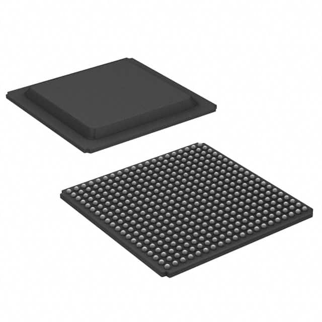
Package and Quantity
XC3S400AN-4FG400I is available in a FG400 package. The quantity may vary depending on the supplier or manufacturer.
Specifications
- Logic Cells: 400,000
- Block RAM: 1,728 Kbits
- DSP Slices: 240
- Maximum Frequency: 400 MHz
- I/O Pins: 400
- Operating Voltage: 1.2V
Pin Configuration
The detailed pin configuration of XC3S400AN-4FG400I can be found in the product datasheet. It provides information about the specific functions and connections of each pin.
Functional Features
XC3S400AN-4FG400I offers several functional features that enhance its usability:
- Configurable Logic Blocks (CLBs): These blocks consist of Look-Up Tables (LUTs) and flip-flops, allowing users to implement custom logic functions.
- Digital Signal Processing (DSP) Slices: These dedicated blocks provide hardware acceleration for signal processing tasks, such as filtering and modulation.
- Memory Blocks: The FPGA includes Block RAMs that can be used for data storage or as FIFO buffers.
- Clock Management Tiles (CMTs): These tiles offer flexible clock distribution and phase-locked loop (PLL) capabilities.
- I/O Interfaces: XC3S400AN-4FG400I supports various standard interfaces, including LVCMOS, LVTTL, and differential signaling.
Advantages and Disadvantages
Advantages
- Flexibility: FPGAs allow for the implementation of custom logic functions, providing design flexibility.
- Reconfigurability: The ability to reprogram FPGAs enables rapid prototyping and design iterations.
- Parallel Processing: FPGAs can execute multiple tasks simultaneously, improving overall system performance.
- High Integration: XC3S400AN-4FG400I offers a large number of logic cells, enabling complex designs.
Disadvantages
- Complexity: Designing with FPGAs requires specialized knowledge and expertise.
- Cost: FPGAs can be more expensive compared to other programmable logic devices.
- Power Consumption: While efforts have been made to optimize power efficiency, FPGAs still consume more power compared to application-specific integrated circuits (ASICs).
Working Principles
XC3S400AN-4FG400I operates based on the principles of reconfigurable computing. It consists of an array of configurable logic blocks interconnected through programmable routing resources. Users can define the desired functionality by configuring the interconnections and programming the logic cells within the FPGA.
The configuration data is stored in non-volatile memory and loaded into the FPGA during startup. Once configured, the FPGA performs the desired operations based on the programmed logic.
Application Field Plans
XC3S400AN-4FG400I finds applications in various fields, including:
- Telecommunications: FPGAs are used in base stations, network switches, and routers to handle high-speed data processing and protocol conversion.
- Automotive: FPGAs are employed in advanced driver-assistance systems (ADAS), infotainment systems, and engine control units (ECUs) for improved performance and functionality.
- Aerospace: FPGAs are utilized in satellite communication systems, avionics, and radar systems for their reconfigurability and high-performance capabilities.
- Consumer Electronics: FPGAs can be found in smart TVs, gaming consoles, and digital cameras, enabling advanced image processing and multimedia functionalities.
Alternative Models
There are several alternative models available in the market that offer similar features and capabilities as XC3S400AN-4FG400I. Some notable alternatives include:
- Xilinx Spartan-6 FPGA
- Altera Cyclone IV FPGA
- Lattice ECP5 FPGA
- Microsemi SmartFusion2 FPGA
These alternative models provide a range
Liệt kê 10 câu hỏi và câu trả lời thường gặp liên quan đến ứng dụng XC3S400AN-4FG400I trong giải pháp kỹ thuật
Sure! Here are 10 common questions and answers related to the application of XC3S400AN-4FG400I in technical solutions:
Q: What is XC3S400AN-4FG400I? A: XC3S400AN-4FG400I is a field-programmable gate array (FPGA) from Xilinx, which offers programmable logic and digital signal processing capabilities.
Q: What are the key features of XC3S400AN-4FG400I? A: Some key features include 400,000 system gates, 400 input/output pins, 4-input look-up tables, and support for various I/O standards.
Q: What are the typical applications of XC3S400AN-4FG400I? A: XC3S400AN-4FG400I is commonly used in applications such as industrial automation, telecommunications, automotive electronics, and high-performance computing.
Q: How can XC3S400AN-4FG400I be programmed? A: XC3S400AN-4FG400I can be programmed using Xilinx's Vivado Design Suite or ISE Design Suite software tools.
Q: What programming languages can be used with XC3S400AN-4FG400I? A: XC3S400AN-4FG400I can be programmed using hardware description languages (HDLs) such as VHDL or Verilog.
Q: Can XC3S400AN-4FG400I interface with other components or devices? A: Yes, XC3S400AN-4FG400I supports various communication protocols like SPI, I2C, UART, and Ethernet, allowing it to interface with other components or devices.
Q: What are the power requirements for XC3S400AN-4FG400I? A: XC3S400AN-4FG400I typically operates at a voltage range of 1.14V to 1.26V, with a maximum power consumption of around 2.5W.
Q: Can XC3S400AN-4FG400I be used in safety-critical applications? A: Yes, XC3S400AN-4FG400I can be used in safety-critical applications as long as proper design and verification processes are followed.
Q: Are there any development boards available for XC3S400AN-4FG400I? A: Yes, Xilinx offers development boards like the Spartan-3A Evaluation Kit that can be used for prototyping and testing with XC3S400AN-4FG400I.
Q: Where can I find technical documentation and support for XC3S400AN-4FG400I? A: Technical documentation, datasheets, application notes, and support resources for XC3S400AN-4FG400I can be found on Xilinx's official website or community forums.
Please note that the answers provided here are general and may vary depending on specific requirements and use cases.