

Xem thông số kỹ thuật để biết chi tiết sản phẩm.
XC4VLX60-10FF1148I
Product Overview
Category
The XC4VLX60-10FF1148I belongs to the category of Field Programmable Gate Arrays (FPGAs).
Use
FPGAs are integrated circuits that can be programmed and reprogrammed to perform various digital functions. The XC4VLX60-10FF1148I is specifically designed for high-performance applications.
Characteristics
- High-speed processing capabilities
- Large number of configurable logic blocks
- Flexible and reprogrammable design
- Low power consumption
- High reliability and durability
Package
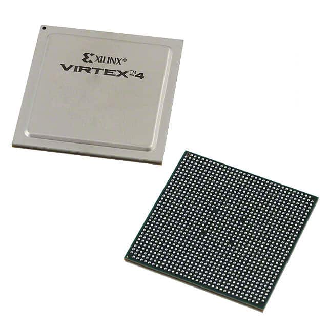
The XC4VLX60-10FF1148I comes in a Flip-Chip 1148-pin package.
Essence
The essence of the XC4VLX60-10FF1148I lies in its ability to provide customizable digital logic functions, allowing designers to implement complex systems on a single chip.
Packaging/Quantity
The XC4VLX60-10FF1148I is typically sold individually or in small quantities, depending on the supplier's packaging options.
Specifications
- FPGA Family: Virtex-4 LX
- Logic Cells: 60,000
- Maximum Number of User I/Os: 648
- Operating Voltage: 1.2V
- Speed Grade: -10
- Package Type: Flip-Chip
- Package Pins: 1148
- Temperature Range: Commercial (0°C to 85°C)
Detailed Pin Configuration
The XC4VLX60-10FF1148I has a total of 1148 pins, each serving a specific purpose in the overall functionality of the FPGA. A detailed pin configuration diagram can be found in the product datasheet provided by the manufacturer.
Functional Features
- Configurable logic blocks for implementing custom digital circuits
- Embedded multipliers for efficient multiplication operations
- High-speed serial transceivers for data communication
- On-chip memory blocks for storing data
- Built-in clock management resources for precise timing control
Advantages and Disadvantages
Advantages
- Flexibility: FPGAs can be reprogrammed to adapt to changing requirements.
- High Performance: The XC4VLX60-10FF1148I offers fast processing capabilities.
- Integration: Multiple digital functions can be implemented on a single chip.
- Low Power Consumption: FPGAs are designed to optimize power usage.
Disadvantages
- Complexity: Designing and programming FPGAs requires specialized knowledge.
- Cost: FPGAs can be more expensive compared to other integrated circuits.
- Limited Resources: The number of logic cells and I/O pins may restrict the complexity of designs.
Working Principles
The XC4VLX60-10FF1148I operates based on the principles of configurable logic. It consists of an array of logic cells that can be interconnected and programmed to perform specific digital functions. These logic cells can be configured using a Hardware Description Language (HDL) or a graphical design tool provided by the FPGA manufacturer. Once programmed, the FPGA executes the desired functionality by routing signals through the configured logic paths.
Detailed Application Field Plans
The XC4VLX60-10FF1148I finds applications in various fields, including:
- Telecommunications: Used in high-speed data transmission systems and network infrastructure equipment.
- Aerospace and Defense: Employed in radar systems, avionics, and military communication devices.
- Industrial Automation: Utilized in control systems, robotics, and machine vision applications.
- Medical Devices: Integrated into medical imaging systems and diagnostic equipment.
- Automotive: Applied in advanced driver assistance systems (ADAS) and infotainment systems.
Detailed and Complete Alternative Models
- XC4VLX100-10FF1148I: A higher-capacity FPGA from the same Virtex-4 LX family, offering 100,000 logic cells.
- XC4VSX35-10FF668C: A lower-cost alternative with 35,000 logic cells and a different package type.
- XC6SLX45-2FGG484C: A newer generation FPGA with 45,000 logic cells and improved power efficiency.
These alternative models provide options with varying capacities, features, and price points to suit different project requirements.
In conclusion, the XC4VLX60-10FF1148I is a high-performance FPGA that offers flexibility, speed, and reliability for a wide range of digital design applications. Its configurable nature and extensive pin configuration make it a versatile choice for designers seeking customizable solutions.
Liệt kê 10 câu hỏi và câu trả lời thường gặp liên quan đến ứng dụng XC4VLX60-10FF1148I trong giải pháp kỹ thuật
Sure! Here are 10 common questions and answers related to the application of XC4VLX60-10FF1148I in technical solutions:
Question: What is XC4VLX60-10FF1148I?
- Answer: XC4VLX60-10FF1148I is a field-programmable gate array (FPGA) from Xilinx, which offers high-performance and flexibility for various technical applications.Question: What are the key features of XC4VLX60-10FF1148I?
- Answer: Some key features of XC4VLX60-10FF1148I include 60,000 logic cells, 1.2V core voltage, 10ns minimum clock period, and support for various I/O standards.Question: What are the typical applications of XC4VLX60-10FF1148I?
- Answer: XC4VLX60-10FF1148I is commonly used in applications such as telecommunications, networking, industrial automation, image processing, and high-performance computing.Question: How can XC4VLX60-10FF1148I be programmed?
- Answer: XC4VLX60-10FF1148I can be programmed using Xilinx's Vivado Design Suite or ISE Design Suite software tools, which provide a graphical interface for designing and implementing FPGA designs.Question: Can XC4VLX60-10FF1148I be reprogrammed multiple times?
- Answer: Yes, XC4VLX60-10FF1148I is a reprogrammable FPGA, allowing users to modify and reconfigure the design multiple times as per their requirements.Question: What are the power requirements for XC4VLX60-10FF1148I?
- Answer: XC4VLX60-10FF1148I requires a 1.2V core voltage and has various power supply pins for different voltage levels, as specified in the datasheet.Question: Does XC4VLX60-10FF1148I support different I/O standards?
- Answer: Yes, XC4VLX60-10FF1148I supports various I/O standards such as LVCMOS, LVTTL, LVDS, SSTL, HSTL, and differential signaling.Question: Can XC4VLX60-10FF1148I interface with external memory devices?
- Answer: Yes, XC4VLX60-10FF1148I has dedicated memory interfaces, including DDR, DDR2, DDR3, and QDR, allowing it to interface with external memory devices.Question: What is the maximum operating frequency of XC4VLX60-10FF1148I?
- Answer: The maximum operating frequency of XC4VLX60-10FF1148I is 10ns (100MHz), which means it can perform operations at a clock speed of up to 100 million cycles per second.Question: Are there any development boards available for XC4VLX60-10FF1148I?
- Answer: Yes, Xilinx offers development boards like the ML605 or KC705, which are specifically designed to work with XC4VLX60-10FF1148I and provide a platform for prototyping and testing applications.
Please note that the answers provided here are general and may vary based on specific requirements and use cases. It's always recommended to refer to the official documentation and datasheets for accurate and detailed information about XC4VLX60-10FF1148I.