

Xem thông số kỹ thuật để biết chi tiết sản phẩm.
XC6SLX100T-3FGG900C
Product Overview
Category
The XC6SLX100T-3FGG900C belongs to the category of Field Programmable Gate Arrays (FPGAs).
Use
FPGAs are integrated circuits that can be programmed after manufacturing. They are widely used in various applications such as digital signal processing, telecommunications, automotive, and aerospace industries.
Characteristics
The XC6SLX100T-3FGG900C is known for its high performance and versatility. It offers a large number of logic cells, on-chip memory, and programmable interconnects, allowing for complex digital designs.
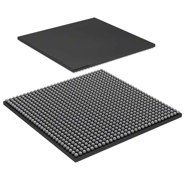
Package
The XC6SLX100T-3FGG900C comes in a FG900 package, which refers to a Fine-Pitch Ball Grid Array (BGA) package with 900 balls. This package provides a compact and reliable solution for mounting the FPGA onto a printed circuit board.
Essence
The essence of the XC6SLX100T-3FGG900C lies in its ability to provide reconfigurable hardware that can be customized for specific applications. It allows designers to implement complex digital systems without the need for custom-designed integrated circuits.
Packaging/Quantity
The XC6SLX100T-3FGG900C is typically sold in trays or reels, depending on the manufacturer's packaging standards. The quantity per package may vary, but it is commonly available in quantities suitable for both prototyping and production purposes.
Specifications
- Logic Cells: 101,261
- Block RAM: 4,860 Kbits
- DSP Slices: 240
- Maximum Frequency: 550 MHz
- I/O Pins: 500
- Operating Voltage: 1.2V
Detailed Pin Configuration
The XC6SLX100T-3FGG900C has a total of 500 I/O pins, which are used for input and output connections. These pins are organized into banks, each with its own voltage requirements and capabilities. The pin configuration can be found in the manufacturer's datasheet.
Functional Features
The XC6SLX100T-3FGG900C offers several functional features that make it a versatile FPGA for various applications:
- High Logic Capacity: With over 100,000 logic cells, this FPGA can handle complex digital designs.
- Flexible Interconnects: The programmable interconnects allow for easy routing of signals between different components within the FPGA.
- On-Chip Memory: The built-in block RAM provides fast and efficient memory access for data storage and retrieval.
- DSP Slices: The dedicated Digital Signal Processing (DSP) slices enable efficient implementation of mathematical operations commonly used in signal processing applications.
Advantages and Disadvantages
Advantages
- Versatility: The reconfigurable nature of FPGAs allows for flexibility in design and adaptation to changing requirements.
- Rapid Prototyping: FPGAs enable quick development and testing of digital systems without the need for custom silicon.
- Cost-Effective: FPGAs eliminate the need for expensive custom-designed integrated circuits, reducing overall production costs.
Disadvantages
- Power Consumption: FPGAs tend to consume more power compared to application-specific integrated circuits (ASICs).
- Complexity: Designing for FPGAs requires specialized knowledge and tools, making it more challenging for beginners.
- Limited Performance: While FPGAs offer high performance, they may not match the speed and efficiency of dedicated ASICs for specific tasks.
Working Principles
FPGAs like the XC6SLX100T-3FGG900C consist of an array of configurable logic blocks interconnected through programmable routing resources. These logic blocks can be programmed to perform specific functions, and the interconnects can be configured to route signals between different blocks. The configuration of the FPGA is stored in memory cells, which can be reprogrammed as needed.
When powered on, the FPGA loads its configuration from an external memory device or through a dedicated configuration interface. Once configured, the FPGA operates based on the programmed logic and routing, allowing for the desired functionality.
Detailed Application Field Plans
The XC6SLX100T-3FGG900C finds applications in various fields, including:
- Digital Signal Processing: FPGAs are commonly used in signal processing applications such as audio and video processing, radar systems, and wireless communication.
- Embedded Systems: FPGAs can be utilized in embedded systems for tasks like motor control, sensor interfacing, and real-time data processing.
- High-Performance Computing: FPGAs are increasingly being used in high-performance computing environments to accelerate specific algorithms and computations.
- Prototyping and Development: FPGAs provide a platform for rapid prototyping and development of digital systems before transitioning to custom-designed ASICs.
Detailed and Complete Alternative Models
- XC7
Liệt kê 10 câu hỏi và câu trả lời thường gặp liên quan đến ứng dụng XC6SLX100T-3FGG900C trong giải pháp kỹ thuật
Sure! Here are 10 common questions and answers related to the application of XC6SLX100T-3FGG900C in technical solutions:
Question: What is XC6SLX100T-3FGG900C?
- Answer: XC6SLX100T-3FGG900C is a field-programmable gate array (FPGA) from Xilinx, which is commonly used in various technical solutions.Question: What are the key features of XC6SLX100T-3FGG900C?
- Answer: Some key features of XC6SLX100T-3FGG900C include a high logic capacity, advanced DSP capabilities, multiple I/O standards, and low power consumption.Question: In what applications can XC6SLX100T-3FGG900C be used?
- Answer: XC6SLX100T-3FGG900C can be used in a wide range of applications such as telecommunications, industrial automation, aerospace, defense, and scientific research.Question: How does XC6SLX100T-3FGG900C differ from other FPGAs?
- Answer: XC6SLX100T-3FGG900C offers a balance between logic capacity, performance, and power consumption, making it suitable for many different applications. It also has specific features like integrated memory blocks and high-speed serial transceivers.Question: What development tools are available for programming XC6SLX100T-3FGG900C?
- Answer: Xilinx provides software tools like Vivado Design Suite and ISE Design Suite for programming and configuring XC6SLX100T-3FGG900C.Question: Can XC6SLX100T-3FGG900C be used in safety-critical applications?
- Answer: Yes, XC6SLX100T-3FGG900C can be used in safety-critical applications. However, additional measures like redundancy and fault-tolerant design may be required to ensure reliability.Question: What is the power consumption of XC6SLX100T-3FGG900C?
- Answer: The power consumption of XC6SLX100T-3FGG900C depends on various factors such as the configuration, operating frequency, and utilization. It is recommended to refer to the datasheet for detailed power specifications.Question: Can XC6SLX100T-3FGG900C interface with other components or devices?
- Answer: Yes, XC6SLX100T-3FGG900C supports various I/O standards and can interface with other components or devices such as sensors, memory modules, communication interfaces, and more.Question: Are there any limitations or constraints when using XC6SLX100T-3FGG900C?
- Answer: XC6SLX100T-3FGG900C has certain limitations like limited logic resources, finite number of I/O pins, and specific voltage requirements. These should be considered during the design phase.Question: Where can I find more information about XC6SLX100T-3FGG900C?
- Answer: You can find more information about XC6SLX100T-3FGG900C on Xilinx's official website, including datasheets, application notes, user guides, and technical support resources.