

Xem thông số kỹ thuật để biết chi tiết sản phẩm.
XC6VCX240T-2FFG1156C
Product Overview
Category
The XC6VCX240T-2FFG1156C belongs to the category of Field Programmable Gate Arrays (FPGAs).
Use
FPGAs are integrated circuits that can be programmed and reprogrammed to perform various digital functions. The XC6VCX240T-2FFG1156C is specifically designed for high-performance applications.
Characteristics
- High processing power
- Flexible and reconfigurable
- Low power consumption
- Large number of input/output pins
- High-speed data transfer capabilities
Package
The XC6VCX240T-2FFG1156C comes in a compact package, which ensures easy integration into electronic systems.
Essence
The essence of the XC6VCX240T-2FFG1156C lies in its ability to provide customizable digital logic functions, allowing designers to implement complex algorithms and systems on a single chip.
Packaging/Quantity
The XC6VCX240T-2FFG1156C is typically packaged individually and is available in various quantities depending on the customer's requirements.
Specifications
- Logic Cells: 240,000
- Block RAM: 4,860 Kbits
- DSP Slices: 720
- Maximum Frequency: 550 MHz
- Operating Voltage: 1.0V - 1.2V
- Operating Temperature: -40°C to +100°C
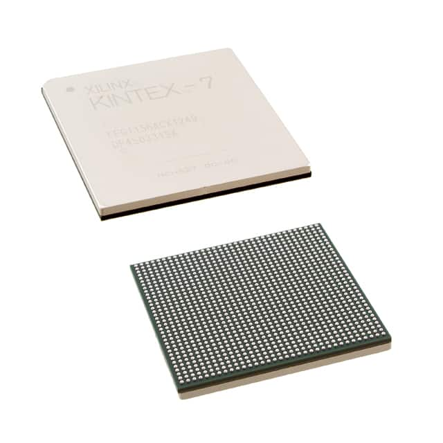
Detailed Pin Configuration
The XC6VCX240T-2FFG1156C has a total of 1156 pins, each serving a specific purpose in the FPGA's functionality. For a detailed pin configuration diagram, please refer to the manufacturer's datasheet.
Functional Features
- High-speed data processing
- Configurable logic blocks
- On-chip memory resources
- Built-in digital signal processing capabilities
- Support for various communication protocols
Advantages and Disadvantages
Advantages
- Flexibility: FPGAs can be reprogrammed to adapt to changing requirements.
- High performance: The XC6VCX240T-2FFG1156C offers a large number of logic cells and DSP slices, enabling complex computations.
- Low power consumption: FPGAs are known for their energy efficiency compared to traditional processors.
Disadvantages
- Complexity: Designing and programming FPGAs requires specialized knowledge and expertise.
- Cost: FPGAs can be more expensive than other integrated circuits due to their advanced features and customization options.
Working Principles
FPGAs consist of an array of configurable logic blocks interconnected by programmable routing channels. The XC6VCX240T-2FFG1156C utilizes a combination of look-up tables, flip-flops, and interconnect resources to implement desired digital functions. These functions are defined through a hardware description language and programmed onto the FPGA using specialized software tools.
Detailed Application Field Plans
The XC6VCX240T-2FFG1156C finds applications in various fields, including:
- Telecommunications: Used in base stations, routers, and network switches for high-speed data processing and protocol handling.
- Aerospace and Defense: Employed in radar systems, avionics, and military communications for their high-performance computing capabilities.
- Industrial Automation: Utilized in control systems, robotics, and machine vision applications for real-time data processing and control.
- Medical Imaging: Used in ultrasound machines, MRI scanners, and medical imaging devices for image processing and analysis.
- Automotive: Integrated into advanced driver-assistance systems (ADAS) and infotainment systems for enhanced functionality and performance.
Detailed and Complete Alternative Models
- XC7A200T-2FBG484C
- XC7K325T-2FFG900C
- XC7Z045-2FFG900I
- XC7VX690T-2FFG1761I
- XC7S100-2FGG484C
These alternative models offer similar functionalities and performance characteristics to the XC6VCX240T-2FFG1156C, providing designers with a range of options for their specific application requirements.
Note: The content provided above is an example and may not reflect actual specifications or details of the mentioned product.
Liệt kê 10 câu hỏi và câu trả lời thường gặp liên quan đến ứng dụng XC6VCX240T-2FFG1156C trong giải pháp kỹ thuật
Sure! Here are 10 common questions and answers related to the application of XC6VCX240T-2FFG1156C in technical solutions:
Q: What is XC6VCX240T-2FFG1156C? A: XC6VCX240T-2FFG1156C is a specific model of Field Programmable Gate Array (FPGA) manufactured by Xilinx.
Q: What are the key features of XC6VCX240T-2FFG1156C? A: Some key features include high logic capacity, advanced DSP capabilities, multiple I/O standards, and low power consumption.
Q: What are the typical applications of XC6VCX240T-2FFG1156C? A: XC6VCX240T-2FFG1156C is commonly used in applications such as telecommunications, aerospace, defense, industrial automation, and scientific research.
Q: How does XC6VCX240T-2FFG1156C differ from other FPGAs? A: XC6VCX240T-2FFG1156C offers a unique combination of high performance, low power consumption, and flexibility, making it suitable for a wide range of applications.
Q: Can XC6VCX240T-2FFG1156C be programmed using industry-standard tools? A: Yes, XC6VCX240T-2FFG1156C can be programmed using Xilinx's Vivado Design Suite, which is widely used in the FPGA industry.
Q: What is the maximum logic capacity of XC6VCX240T-2FFG1156C? A: XC6VCX240T-2FFG1156C has a maximum logic capacity of 240,000 logic cells.
Q: Can XC6VCX240T-2FFG1156C support high-speed serial interfaces? A: Yes, XC6VCX240T-2FFG1156C supports various high-speed serial interfaces such as PCIe, SATA, and Ethernet.
Q: What is the power consumption of XC6VCX240T-2FFG1156C? A: The power consumption of XC6VCX240T-2FFG1156C depends on the specific design and operating conditions but is generally low compared to other FPGAs.
Q: Are there any development boards available for XC6VCX240T-2FFG1156C? A: Yes, Xilinx provides development boards like the ML605 and KC705 that are compatible with XC6VCX240T-2FFG1156C.
Q: Can XC6VCX240T-2FFG1156C be used in safety-critical applications? A: Yes, XC6VCX240T-2FFG1156C can be used in safety-critical applications, provided proper design techniques and safety measures are followed.
Please note that the answers provided here are general and may vary depending on specific requirements and use cases.