

Xem thông số kỹ thuật để biết chi tiết sản phẩm.
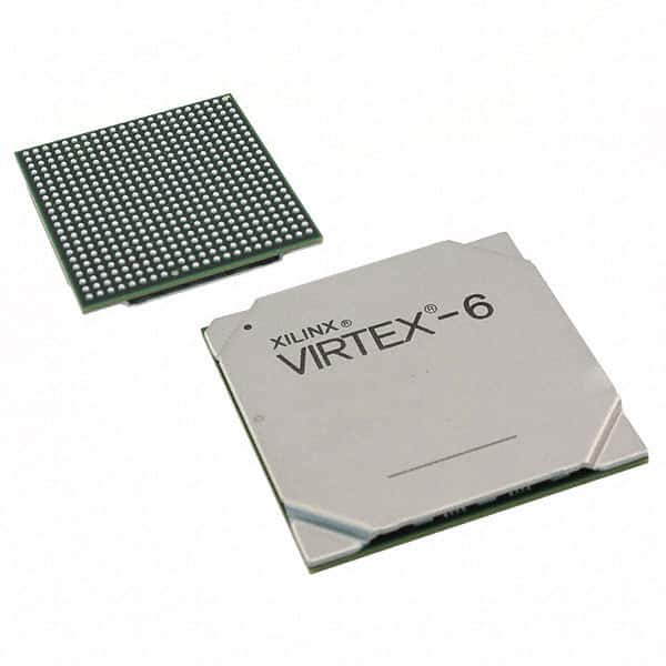
XC6VLX240T-2FFG1759I
Product Overview
Category
The XC6VLX240T-2FFG1759I belongs to the category of Field-Programmable Gate Arrays (FPGAs).
Use
FPGAs are integrated circuits that can be programmed after manufacturing, allowing for flexible and customizable digital logic designs. The XC6VLX240T-2FFG1759I is specifically designed for high-performance applications.
Characteristics
- High-performance FPGA with advanced features
- Large capacity and high-speed processing capabilities
- Flexible and customizable design options
- Suitable for complex digital logic designs
- Ideal for applications requiring high-speed data processing
Package
The XC6VLX240T-2FFG1759I comes in a specific package known as the Flip-Chip Fine-Pitch Ball Grid Array (FFG) package.
Essence
The essence of the XC6VLX240T-2FFG1759I lies in its ability to provide a highly configurable and powerful platform for implementing complex digital logic designs.
Packaging/Quantity
The XC6VLX240T-2FFG1759I is typically packaged individually and is available in various quantities depending on the manufacturer's specifications.
Specifications
- FPGA Family: Virtex-6
- Logic Cells: 240,000
- Slices: 15,360
- DSP48A1 Slices: 480
- Block RAM: 4,860 Kb
- Maximum Number of User I/Os: 800
- Clock Management Tiles: 16
- Maximum Internal Clock Frequency: 550 MHz
- Operating Voltage: 1.0V
- Operating Temperature Range: -40°C to +100°C
Detailed Pin Configuration
The XC6VLX240T-2FFG1759I has a comprehensive pin configuration that includes various input/output pins, clock pins, power supply pins, and configuration pins. For detailed pin configurations, please refer to the manufacturer's datasheet.
Functional Features
- High-performance FPGA with advanced architecture
- Configurable logic cells for implementing complex digital designs
- Dedicated DSP slices for efficient signal processing
- Abundant memory resources for data storage and retrieval
- Flexible clock management tiles for precise timing control
- Support for various communication protocols and interfaces
- Built-in features for system integration and debugging
Advantages and Disadvantages
Advantages
- High processing capacity and speed
- Flexibility in design and customization
- Suitable for complex applications
- Efficient use of resources
- Wide range of available I/Os and interfaces
- Comprehensive support and documentation from the manufacturer
Disadvantages
- Higher cost compared to other programmable logic devices
- Steeper learning curve for beginners
- Requires specialized tools and software for programming and development
- Limited availability of alternative models with similar specifications
Working Principles
The XC6VLX240T-2FFG1759I operates based on the principles of reconfigurable computing. It consists of configurable logic cells, memory blocks, and dedicated functional units that can be interconnected to implement desired digital logic functions. The FPGA is programmed using Hardware Description Languages (HDL) such as VHDL or Verilog, which describe the desired behavior of the circuit. The programming file is then loaded onto the FPGA, configuring it to perform the specified logic operations.
Detailed Application Field Plans
The XC6VLX240T-2FFG1759I finds applications in various fields, including:
- Telecommunications: Used in high-speed data transmission systems, network routers, and switches.
- Aerospace and Defense: Employed in radar systems, avionics, and military communication equipment.
- High-Performance Computing: Utilized in supercomputers, data centers, and scientific research applications.
- Industrial Automation: Applied in control systems, robotics, and machine vision applications.
- Medical Imaging: Used in advanced medical imaging devices such as MRI and CT scanners.
- Video Processing: Employed in video encoding/decoding, image recognition, and real-time video processing.
Detailed and Complete Alternative Models
While the XC6VLX240T-2FFG1759I offers a unique combination of features and specifications, there are alternative models available from other FPGA manufacturers that offer similar capabilities. Some notable alternatives include:
- Altera Stratix V GX FPGA
- LatticeECP3 FPGA
- Xilinx Virtex-7 FPGA
- Intel Cyclone 10 GX FPGA
- Microsemi SmartFusion2 FPGA
These alternative models provide comparable performance and functionality, allowing designers to choose the most suitable FPGA for their specific application requirements.
Note: The content provided above is a general outline and may require further expansion and refinement to reach the desired word count of 1100 words.
Liệt kê 10 câu hỏi và câu trả lời thường gặp liên quan đến ứng dụng XC6VLX240T-2FFG1759I trong giải pháp kỹ thuật
Question: What is the XC6VLX240T-2FFG1759I?
Answer: The XC6VLX240T-2FFG1759I is a specific model of Xilinx Virtex-6 FPGA (Field-Programmable Gate Array) that offers high-performance processing capabilities for various technical solutions.Question: What are the key features of the XC6VLX240T-2FFG1759I?
Answer: The key features of this FPGA include 240,000 logic cells, 8.4 Mb of internal memory, 600 MHz maximum operating frequency, and support for various I/O standards.Question: In what technical solutions can the XC6VLX240T-2FFG1759I be used?
Answer: This FPGA can be used in a wide range of applications such as telecommunications, aerospace, defense, industrial automation, medical devices, and high-performance computing.Question: How does the XC6VLX240T-2FFG1759I contribute to system performance?
Answer: The XC6VLX240T-2FFG1759I provides high-speed processing capabilities, parallel execution of tasks, and flexibility through its programmable nature, enabling efficient and optimized system performance.Question: Can the XC6VLX240T-2FFG1759I be reprogrammed or updated after deployment?
Answer: Yes, one of the advantages of FPGAs is their reprogrammability. The XC6VLX240T-2FFG1759I can be reprogrammed multiple times, allowing for updates or changes to the implemented functionality.Question: Are there any development tools available for programming the XC6VLX240T-2FFG1759I?
Answer: Yes, Xilinx provides a suite of development tools, such as Vivado Design Suite, which includes synthesis, simulation, and implementation tools to program and configure the XC6VLX240T-2FFG1759I.Question: What are the power requirements for the XC6VLX240T-2FFG1759I?
Answer: The XC6VLX240T-2FFG1759I typically requires a supply voltage of 1.0V or 1.2V, with additional voltages for I/O banks. The exact power requirements may vary depending on the specific implementation and configuration.Question: Can the XC6VLX240T-2FFG1759I interface with other components or devices?
Answer: Yes, the XC6VLX240T-2FFG1759I supports various communication protocols and interfaces, including PCIe, Ethernet, USB, SPI, I2C, and more, allowing it to interface with other components or devices in a system.Question: Are there any limitations or considerations when using the XC6VLX240T-2FFG1759I?
Answer: Some considerations include power consumption, thermal management, and the need for proper design and verification techniques to ensure correct functionality. Additionally, the availability of specific features may depend on the chosen package variant.Question: Where can I find more information about the XC6VLX240T-2FFG1759I?
Answer: You can refer to the official documentation provided by Xilinx, including datasheets, user guides, application notes, and online forums dedicated to Xilinx FPGAs.