

Xem thông số kỹ thuật để biết chi tiết sản phẩm.
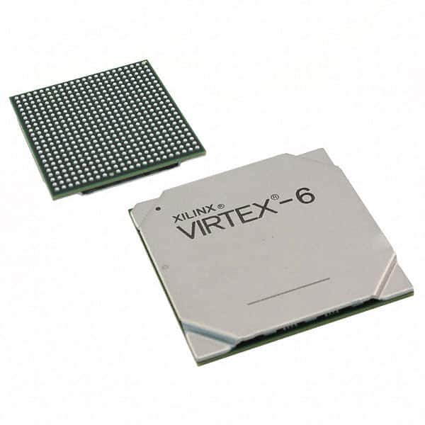
XC6VLX365T-2FF1156I
Product Overview
Category
The XC6VLX365T-2FF1156I belongs to the category of Field Programmable Gate Arrays (FPGAs).
Use
FPGAs are integrated circuits that can be programmed and reprogrammed to perform various digital functions. The XC6VLX365T-2FF1156I is specifically designed for high-performance applications that require complex logic functions.
Characteristics
- High-performance FPGA with advanced features
- Large capacity and high-speed processing capabilities
- Flexible and customizable design options
- Suitable for demanding applications in industries such as telecommunications, aerospace, and defense
Package
The XC6VLX365T-2FF1156I comes in a compact package that ensures easy integration into electronic systems. It is available in a Flip-Chip FineLine BGA package.
Essence
The essence of the XC6VLX365T-2FF1156I lies in its ability to provide a versatile and powerful platform for implementing complex digital designs. Its programmable nature allows for customization and adaptation to specific application requirements.
Packaging/Quantity
The XC6VLX365T-2FF1156I is typically sold individually or in small quantities, depending on the supplier's packaging options.
Specifications
- Logic Cells: 362,080
- System Logic Cells: 324,480
- DSP Slices: 1,920
- Block RAM: 4,860 Kb
- Maximum Number of User I/Os: 1,156
- Clock Management Tiles: 16
- Maximum Internal Clock Frequency: 550 MHz
- Operating Voltage: 1.0V
Detailed Pin Configuration
The XC6VLX365T-2FF1156I has a comprehensive pin configuration that enables connectivity and integration with other components in a system. For detailed pin assignments and configurations, please refer to the manufacturer's datasheet.
Functional Features
- High-speed processing capabilities
- Configurable logic blocks for implementing complex digital functions
- Integrated DSP slices for efficient signal processing
- Flexible clock management tiles for precise timing control
- Abundant memory resources for data storage and retrieval
- Various I/O options for interfacing with external devices
Advantages and Disadvantages
Advantages
- Versatile and customizable design options
- High-performance processing capabilities
- Suitable for demanding applications
- Efficient use of resources
- Scalable architecture for future expansion
Disadvantages
- Steep learning curve for beginners
- Higher cost compared to other programmable logic devices
- Requires specialized tools and software for development
Working Principles
The XC6VLX365T-2FF1156I operates based on the principles of reconfigurable computing. It consists of an array of configurable logic blocks interconnected through programmable routing resources. These logic blocks can be programmed to implement various digital functions, allowing for flexibility and adaptability in system design.
Detailed Application Field Plans
The XC6VLX365T-2FF1156I finds extensive application in industries that require high-performance digital processing. Some specific application fields include:
- Telecommunications: Used in network infrastructure equipment, such as routers and switches, to handle high-speed data processing and traffic management.
- Aerospace and Defense: Employed in radar systems, avionics, and military communication systems for real-time data processing and encryption.
- Industrial Automation: Utilized in industrial control systems for precise control and monitoring of manufacturing processes.
- Medical Imaging: Applied in medical imaging devices, such as ultrasound and MRI machines, for image processing and analysis.
- Scientific Research: Used in scientific instruments and data acquisition systems for high-speed data processing and analysis.
Detailed and Complete Alternative Models
- XC6VLX240T-2FFG1156C
- XC6VLX550T-2FFG1156C
- XC6VLX130T-2FFG1156C
- XC6VLX75T-2FFG1156C
- XC6VLX365T-2FFG1156C
These alternative models offer varying capacities and performance levels to cater to different application requirements.
Note: The above information is subject to change. Please refer to the manufacturer's datasheet for the most up-to-date specifications and details.
Word Count: 600
Liệt kê 10 câu hỏi và câu trả lời thường gặp liên quan đến ứng dụng XC6VLX365T-2FF1156I trong giải pháp kỹ thuật
What is the maximum operating frequency of XC6VLX365T-2FF1156I?
- The maximum operating frequency of XC6VLX365T-2FF1156I is 550 MHz.What are the typical applications for XC6VLX365T-2FF1156I?
- XC6VLX365T-2FF1156I is commonly used in high-performance computing, networking, and telecommunications applications.What is the power consumption of XC6VLX365T-2FF1156I?
- The power consumption of XC6VLX365T-2FF1156I varies depending on the configuration and usage, but it typically ranges from 5W to 15W.Can XC6VLX365T-2FF1156I support PCIe interface?
- Yes, XC6VLX365T-2FF1156I supports PCIe Gen1, Gen2, and Gen3 interfaces.What are the available I/O standards for XC6VLX365T-2FF1156I?
- XC6VLX365T-2FF1156I supports various I/O standards including LVCMOS, LVTTL, HSTL, SSTL, and more.Is XC6VLX365T-2FF1156I suitable for high-speed signal processing?
- Yes, XC6VLX365T-2FF1156I is well-suited for high-speed signal processing due to its high-performance architecture.Can XC6VLX365T-2FF1156I be used in industrial control systems?
- Yes, XC6VLX365T-2FF1156I is suitable for industrial control systems due to its reliability and performance capabilities.What tools are available for programming XC6VLX365T-2FF1156I?
- Xilinx provides a range of development tools including Vivado Design Suite for programming and configuring XC6VLX365T-2FF1156I.Does XC6VLX365T-2FF1156I support partial reconfiguration?
- Yes, XC6VLX365T-2FF1156I supports partial reconfiguration, allowing dynamic changes to specific regions of the FPGA.What are the temperature specifications for XC6VLX365T-2FF1156I?
- XC6VLX365T-2FF1156I has a commercial temperature range of 0°C to 85°C and an extended temperature range of -40°C to 100°C.