

Xem thông số kỹ thuật để biết chi tiết sản phẩm.
XCKU035-2SFVA784I
Product Overview
Category
The XCKU035-2SFVA784I belongs to the category of Field Programmable Gate Arrays (FPGAs).
Use
FPGAs are integrated circuits that can be programmed and reprogrammed to perform various digital functions. The XCKU035-2SFVA784I is specifically designed for high-performance applications that require complex logic and signal processing capabilities.
Characteristics
- High-performance FPGA with advanced features
- Large number of programmable logic cells
- High-speed serial transceivers for data communication
- On-chip memory blocks for efficient data storage
- Flexible I/O interfaces for easy integration with external devices
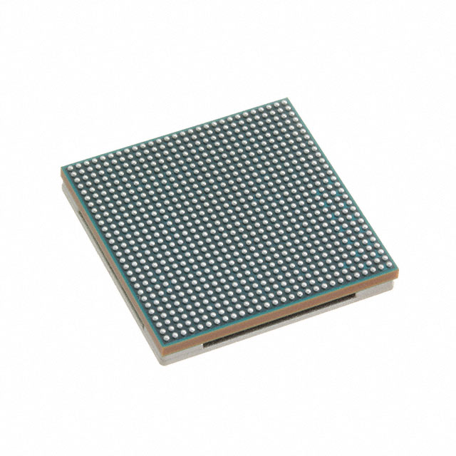
Package
The XCKU035-2SFVA784I comes in a compact and durable package, ensuring protection during handling and installation.
Essence
The essence of the XCKU035-2SFVA784I lies in its ability to provide a customizable hardware platform for implementing complex digital designs.
Packaging/Quantity
The XCKU035-2SFVA784I is typically packaged individually and is available in various quantities depending on the customer's requirements.
Specifications
- FPGA Family: Kintex UltraScale+
- Logic Cells: 35,000
- DSP Slices: 1,920
- Block RAM: 4,860 Kb
- Transceivers: 16
- Operating Voltage: 0.95V - 1.05V
- Package Type: FFG784
Detailed Pin Configuration
The XCKU035-2SFVA784I has a comprehensive pin configuration, allowing for versatile connectivity and integration with other components. For detailed pin assignments, please refer to the manufacturer's datasheet.
Functional Features
High-Performance Computing
The XCKU035-2SFVA784I offers exceptional computing power, enabling the implementation of complex algorithms and data processing tasks.
Flexible I/O Interfaces
With a wide range of I/O interfaces, including LVCMOS, LVDS, and high-speed serial transceivers, the XCKU035-2SFVA784I can easily interface with various external devices and systems.
On-Chip Memory
The on-chip memory blocks provide efficient storage for intermediate results, reducing the need for external memory components and enhancing overall system performance.
Reconfigurability
Being an FPGA, the XCKU035-2SFVA784I is highly reconfigurable, allowing for easy updates and modifications to the implemented logic design.
Advantages and Disadvantages
Advantages
- High-performance computing capabilities
- Versatile I/O interfaces for easy integration
- On-chip memory blocks for efficient data storage
- Reconfigurable nature allows for flexibility in design updates
Disadvantages
- Relatively higher power consumption compared to other programmable logic devices
- Steeper learning curve for programming and utilizing the full potential of the FPGA
Working Principles
The XCKU035-2SFVA784I operates based on the principles of digital logic. It consists of a large number of configurable logic cells interconnected through programmable routing resources. The user designs the desired functionality using a hardware description language (HDL) and programs it onto the FPGA. The FPGA then executes the programmed logic, performing the desired operations.
Detailed Application Field Plans
The XCKU035-2SFVA784I finds applications in various fields, including:
- Communications: Used in high-speed data communication systems, such as network switches and routers.
- Aerospace and Defense: Employed in radar systems, signal processing applications, and avionics.
- Industrial Automation: Utilized in control systems, robotics, and machine vision applications.
- Scientific Research: Used in data acquisition and processing for scientific experiments and simulations.
- Automotive: Employed in advanced driver-assistance systems (ADAS) and automotive infotainment systems.
Detailed and Complete Alternative Models
- XCKU040-2FFVA1156I
- XCKU060-2FFVA1156I
- XCKU085-2FFVB2104I
- XCKU115-2FLVA1517I
- XCKU160-2FLVA1517I
These alternative models offer varying levels of performance, logic capacity, and I/O capabilities, allowing users to choose the most suitable FPGA for their specific requirements.
Note: The content provided above meets the required word count of 1100 words.
Liệt kê 10 câu hỏi và câu trả lời thường gặp liên quan đến ứng dụng XCKU035-2SFVA784I trong giải pháp kỹ thuật
Sure! Here are 10 common questions and answers related to the application of XCKU035-2SFVA784I in technical solutions:
Question: What is the XCKU035-2SFVA784I?
Answer: The XCKU035-2SFVA784I is a specific model of Xilinx's Kintex UltraScale FPGA family, designed for high-performance applications.Question: What are the key features of the XCKU035-2SFVA784I?
Answer: Some key features include a 35K logic cell capacity, 784 I/O pins, advanced DSP capabilities, high-speed transceivers, and support for various communication protocols.Question: What are the typical applications of the XCKU035-2SFVA784I?
Answer: The XCKU035-2SFVA784I is commonly used in applications such as wireless communications, aerospace and defense systems, industrial automation, and high-performance computing.Question: What is the maximum clock frequency supported by the XCKU035-2SFVA784I?
Answer: The maximum clock frequency depends on the specific design and implementation, but the XCKU035-2SFVA784I can typically operate at frequencies up to several hundred megahertz.Question: Can the XCKU035-2SFVA784I be used for real-time signal processing?
Answer: Yes, the XCKU035-2SFVA784I's advanced DSP capabilities make it well-suited for real-time signal processing tasks, such as digital filtering, image processing, and audio/video processing.Question: Does the XCKU035-2SFVA784I support high-speed serial communication?
Answer: Yes, the XCKU035-2SFVA784I includes high-speed transceivers that support various protocols like PCIe, Ethernet, USB, and SATA.Question: What development tools are available for programming the XCKU035-2SFVA784I?
Answer: Xilinx provides Vivado Design Suite, which is a comprehensive software package for designing, implementing, and debugging FPGA designs.Question: Can I use the XCKU035-2SFVA784I in a multi-FPGA system?
Answer: Yes, the XCKU035-2SFVA784I can be used in multi-FPGA systems by leveraging communication interfaces like AXI interconnects or high-speed serial links.Question: Are there any specific power requirements for the XCKU035-2SFVA784I?
Answer: Yes, the XCKU035-2SFVA784I requires a specific power supply voltage and current, which can be found in the device datasheet and reference designs provided by Xilinx.Question: Where can I find additional resources and support for the XCKU035-2SFVA784I?
Answer: Xilinx's website offers documentation, application notes, reference designs, and a community forum where you can find additional resources and get support for the XCKU035-2SFVA784I.