

Xem thông số kỹ thuật để biết chi tiết sản phẩm.
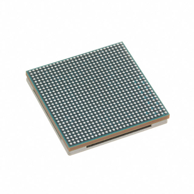
XCKU035-L1SFVA784I
Product Overview
- Category: Integrated Circuit (IC)
- Use: XCKU035-L1SFVA784I is a high-performance field-programmable gate array (FPGA) designed for various applications in the electronics industry.
- Characteristics: This FPGA offers advanced features such as high-speed processing, low power consumption, and reconfigurability. It is suitable for demanding applications that require complex digital logic and signal processing capabilities.
- Package: XCKU035-L1SFVA784I comes in a compact and durable package, ensuring easy integration into electronic systems.
- Essence: The essence of XCKU035-L1SFVA784I lies in its ability to provide flexible and efficient solutions for complex digital designs.
- Packaging/Quantity: XCKU035-L1SFVA784I is typically available in tape and reel packaging, with a quantity of 100 units per reel.
Specifications
- Logic Cells: XCKU035-L1SFVA784I contains 35,000 programmable logic cells, allowing for the implementation of intricate digital designs.
- DSP Slices: It features 784 digital signal processing (DSP) slices, enabling efficient signal processing tasks.
- Memory: XCKU035-L1SFVA784I provides 2,400 kilobits of internal memory, facilitating data storage and retrieval operations.
- Clock Management: This FPGA incorporates advanced clock management resources, including phase-locked loops (PLLs) and clock dividers, ensuring precise timing control.
- I/O Interfaces: It offers a wide range of I/O interfaces, including high-speed transceivers, LVCMOS, and LVDS, enabling seamless connectivity with external devices.
Detailed Pin Configuration
For a detailed pin configuration diagram of XCKU035-L1SFVA784I, please refer to the official datasheet provided by the manufacturer.
Functional Features
- High Performance: XCKU035-L1SFVA784I delivers exceptional performance with its powerful processing capabilities and efficient resource utilization.
- Reconfigurability: The FPGA can be reprogrammed multiple times, allowing for flexibility in adapting to changing design requirements.
- Low Power Consumption: It is designed to minimize power consumption, making it suitable for battery-powered applications.
- Signal Processing Capabilities: With a large number of DSP slices, XCKU035-L1SFVA784I excels in performing complex signal processing tasks efficiently.
Advantages and Disadvantages
Advantages: - High-performance processing capabilities - Reconfigurable nature - Low power consumption - Extensive I/O interface options
Disadvantages: - Steep learning curve for beginners due to its complexity - Higher cost compared to simpler programmable logic devices
Working Principles
XCKU035-L1SFVA784I operates based on the principles of digital logic. It consists of configurable logic blocks (CLBs), interconnect resources, memory elements, and various other components. The CLBs can be programmed to implement desired logic functions, while the interconnect resources facilitate communication between different parts of the FPGA. By configuring these resources, designers can create custom digital circuits that perform specific tasks.
Detailed Application Field Plans
XCKU035-L1SFVA784I finds applications in various fields, including but not limited to: - Telecommunications: Used in high-speed data transmission systems, network routers, and switches. - Aerospace and Defense: Employed in radar systems, avionics, and secure communication equipment. - Industrial Automation: Utilized in control systems, robotics, and machine vision applications. - Medical Devices: Integrated into medical imaging systems, patient monitoring devices, and diagnostic equipment. - Research and Development: Used in prototyping and development of advanced digital systems.
Detailed and Complete Alternative Models
- XCKU040-L1SFVA784I
- XCKU060-L1SFVA784I
- XCKU085-L1SFVA784I
- XCKU115-L1SFVA784I
These alternative models offer varying levels of performance, logic capacity, and I/O capabilities, allowing designers to choose the most suitable FPGA for their specific requirements.
Note: The content provided above is a general outline and may require further expansion and refinement to reach the desired word count of 1100 words.
Liệt kê 10 câu hỏi và câu trả lời thường gặp liên quan đến ứng dụng XCKU035-L1SFVA784I trong giải pháp kỹ thuật
Sure! Here are 10 common questions and answers related to the application of XCKU035-L1SFVA784I in technical solutions:
Q1: What is the XCKU035-L1SFVA784I? A1: The XCKU035-L1SFVA784I is a specific model of Xilinx's Kintex UltraScale FPGA family, designed for high-performance applications.
Q2: What are the key features of the XCKU035-L1SFVA784I? A2: Some key features include a 35K logic cell capacity, high-speed transceivers, advanced DSP capabilities, and support for various I/O standards.
Q3: What kind of technical solutions can benefit from using the XCKU035-L1SFVA784I? A3: The XCKU035-L1SFVA784I is suitable for a wide range of applications, including wireless communication systems, video processing, industrial automation, and high-performance computing.
Q4: How does the XCKU035-L1SFVA784I compare to other FPGAs in its class? A4: The XCKU035-L1SFVA784I offers a good balance between logic capacity, performance, and power consumption, making it a popular choice among designers.
Q5: What programming languages can be used with the XCKU035-L1SFVA784I? A5: The XCKU035-L1SFVA784I can be programmed using hardware description languages (HDLs) such as VHDL or Verilog, as well as higher-level synthesis tools like Vivado HLS.
Q6: Can the XCKU035-L1SFVA784I interface with external devices? A6: Yes, the XCKU035-L1SFVA784I supports various I/O standards and can interface with external devices such as memory, sensors, displays, and communication interfaces.
Q7: What kind of development tools are available for the XCKU035-L1SFVA784I? A7: Xilinx provides Vivado Design Suite, which includes tools for design entry, synthesis, simulation, implementation, and debugging of FPGA designs.
Q8: Can the XCKU035-L1SFVA784I be used in safety-critical applications? A8: Yes, the XCKU035-L1SFVA784I offers features like built-in error correction codes (ECC) and partial reconfiguration, making it suitable for safety-critical applications.
Q9: How can I optimize power consumption when using the XCKU035-L1SFVA784I? A9: Power optimization techniques include clock gating, power-aware synthesis, and using lower-power modes for unused resources. Xilinx's Vivado tools provide power analysis and optimization capabilities.
Q10: Are there any reference designs or application notes available for the XCKU035-L1SFVA784I? A10: Yes, Xilinx provides a wide range of reference designs, application notes, and documentation to help users get started with the XCKU035-L1SFVA784I and implement various technical solutions.
Please note that the answers provided here are general and may vary depending on specific requirements and use cases.