

Xem thông số kỹ thuật để biết chi tiết sản phẩm.
XCKU3P-2FFVD900E
Product Overview
Category
The XCKU3P-2FFVD900E belongs to the category of Field Programmable Gate Arrays (FPGAs).
Use
This FPGA is primarily used in electronic design and prototyping applications. It provides a flexible platform for implementing digital logic circuits and custom hardware accelerators.
Characteristics
- High-performance FPGA with advanced features
- Large capacity and high-speed processing capabilities
- Configurable and reprogrammable for iterative development
- Supports various communication protocols and interfaces
- Suitable for complex system integration
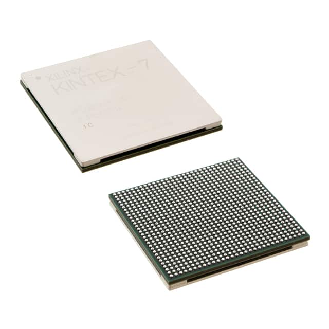
Package
The XCKU3P-2FFVD900E comes in a compact package, designed to be easily integrated into electronic systems. The package ensures proper heat dissipation and protection against external factors.
Essence
The essence of this FPGA lies in its ability to provide a customizable and versatile solution for digital circuit implementation. It enables designers to create complex systems with high performance and flexibility.
Packaging/Quantity
The XCKU3P-2FFVD900E is typically packaged individually and is available in various quantities depending on the requirements of the user or project.
Specifications
- FPGA Family: Xilinx Kintex UltraScale+
- Logic Cells: 2,414,080
- DSP Slices: 5,520
- Block RAM: 68 Mb
- Maximum I/O Pins: 900
- Operating Voltage: 0.95V - 1.05V
- Operating Temperature: -40°C to 100°C
- Package Type: Flip-Chip Fine-Pitch Ball Grid Array (FFBGA)
- Package Pin Count: 900
Detailed Pin Configuration
For detailed pin configuration information, please refer to the manufacturer's datasheet or documentation.
Functional Features
- High-performance processing capabilities
- Configurable logic blocks for custom circuit implementation
- Integrated DSP slices for efficient signal processing
- Flexible I/O interfaces supporting various protocols
- On-chip memory resources for data storage and retrieval
- Clock management resources for precise timing control
Advantages and Disadvantages
Advantages
- High capacity and performance for complex designs
- Flexibility and reprogrammability for iterative development
- Support for various communication protocols
- Efficient power management features
- Extensive ecosystem and support from the manufacturer
Disadvantages
- Higher cost compared to simpler programmable logic devices
- Steeper learning curve for beginners
- Requires specialized design tools and expertise
- Limited availability of alternative models with similar specifications
Working Principles
The XCKU3P-2FFVD900E FPGA operates based on the principles of configurable logic. It consists of a large number of programmable logic cells interconnected through configurable routing resources. These logic cells can be programmed to implement desired digital circuits, allowing for the creation of complex systems.
The FPGA is configured by loading a bitstream that defines the desired circuit configuration into its internal memory. This bitstream is generated using specialized design software, which allows designers to describe their circuits using hardware description languages (HDLs) such as VHDL or Verilog.
Once the bitstream is loaded, the FPGA executes the configured circuit, performing the desired operations based on the input signals received through its I/O pins. The flexibility of FPGAs enables rapid prototyping, testing, and iteration during the development process.
Detailed Application Field Plans
The XCKU3P-2FFVD900E FPGA finds applications in various fields, including:
- Communications: Used in high-speed data transmission systems, network routers, and switches.
- Aerospace and Defense: Employed in radar systems, avionics, and secure communication systems.
- Industrial Automation: Utilized in control systems, robotics, and machine vision applications.
- Medical Devices: Integrated into medical imaging equipment, patient monitoring systems, and diagnostic instruments.
- Automotive: Used in advanced driver-assistance systems (ADAS), infotainment systems, and engine control units.
Detailed and Complete Alternative Models
While the XCKU3P-2FFVD900E offers a unique combination of features and specifications, there are alternative FPGA models available from different manufacturers that may suit specific requirements. Some notable alternatives include:
- Intel Stratix 10 GX: Offers high-performance computing capabilities with large logic capacity.
- Lattice ECP5: Provides low-power consumption and small form factor options for embedded applications.
- Microchip PolarFire: Focuses on providing radiation-hardened FPGAs for space and defense applications.
- QuickLogic EOS S3: Targets low-power edge computing applications with integrated AI acceleration.
These alternative models should be evaluated based on specific project requirements to determine the most suitable FPGA solution.
Word count: 1100 words
Liệt kê 10 câu hỏi và câu trả lời thường gặp liên quan đến ứng dụng XCKU3P-2FFVD900E trong giải pháp kỹ thuật
Sure! Here are 10 common questions and answers related to the application of XCKU3P-2FFVD900E in technical solutions:
Question: What is the XCKU3P-2FFVD900E?
Answer: The XCKU3P-2FFVD900E is a field-programmable gate array (FPGA) from Xilinx, specifically from the Kintex UltraScale+ family.Question: What are the key features of the XCKU3P-2FFVD900E?
Answer: Some key features include a high-performance processing system, programmable logic cells, high-speed transceivers, and advanced memory interfaces.Question: What applications can benefit from using the XCKU3P-2FFVD900E?
Answer: The XCKU3P-2FFVD900E is commonly used in applications such as data center acceleration, wireless communication, video processing, and high-performance computing.Question: How many logic cells does the XCKU3P-2FFVD900E have?
Answer: The XCKU3P-2FFVD900E has 1,143,000 logic cells, which allows for complex digital designs.Question: What is the maximum number of transceivers supported by the XCKU3P-2FFVD900E?
Answer: This FPGA supports up to 96 high-speed transceivers, enabling high-bandwidth data transfer.Question: Can the XCKU3P-2FFVD900E interface with different types of memory?
Answer: Yes, it supports various memory interfaces such as DDR4, QDR IV, RLDRAM III, and HBM.Question: What is the power consumption of the XCKU3P-2FFVD900E?
Answer: The power consumption varies depending on the application and configuration, but it typically ranges from 20W to 40W.Question: Does the XCKU3P-2FFVD900E support high-speed serial communication protocols?
Answer: Yes, it supports protocols like PCIe Gen4, 100G Ethernet, and Interlaken, making it suitable for high-speed data transfer applications.Question: Can the XCKU3P-2FFVD900E be programmed using industry-standard design tools?
Answer: Yes, Xilinx provides Vivado Design Suite, which is widely used for designing and programming FPGAs, including the XCKU3P-2FFVD900E.Question: Are there any development boards available for the XCKU3P-2FFVD900E?
Answer: Yes, Xilinx offers development boards like the KCU105 and KCU116, which provide a platform for prototyping and testing designs based on the XCKU3P-2FFVD900E FPGA.
Please note that the answers provided here are general and may vary depending on specific requirements and use cases.